Home > Press > ULVAC Launches Revolutionary PZT Piezoelectric Thin-film Process Technology and HVM Solution for MEMS Sensors/Actuators: Enabling Reliable, High-quality Film Production for Next Generation Devices
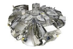 |
| Overhead view of the 8-chamber configuration (7 process chambers and a load-lock chamber) |
Abstract:
ULVAC, Inc. today announced the successful launch of PZT piezoelectric thin-film sputtering technology and a high volume manufacturing (HVM) solution to solve technical issues that have hindered the development of MEMS devices, which are crucial in applications from autonomous driving to next generation wearable terminals (such as smart glasses). The company has begun selling production systems incorporating the new technology.
ULVAC Launches Revolutionary PZT Piezoelectric Thin-film Process Technology and HVM Solution for MEMS Sensors/Actuators: Enabling Reliable, High-quality Film Production for Next Generation Devices
Chigasaki, Japan | Posted on August 16th, 2019Evolutions in technologies such as 5G and AI are expected to accelerate the journey towards smart societies, in which the digitization of all types of industries will improve industrial performance and enhance convenience for people. With increasing levels of multi-functionality found in autonomous driving, AR/VR, security, and smartphone applications, actuators are needed in order to activate devices based on signals received from various types of sensors. Demand for actuators is projected to explode and key issues in their development have come to the fore, including the need for miniaturization, reduced production costs, lower power consumption, and higher performance.
It used to be impossible to fabricate PZT piezoelectric thin films, which constitute the key technology in sensors and actuators, using a low-temperature process with the conventional coating method (Sol-Gel). However, in 2015, ULVAC successfully developed the world's most advanced technology for forming PZT piezoelectric thin films using a low-temperature sputtering process. ULVAC has continued developing this as next-generation MEMS technology.
By further advancing this proprietary technology, ULVAC has reduced running costs by optimizing system operation and has greatly improved the technology's reliability, which is critical for device commercialization. The result is a groundbreaking mass-production technology that is now incorporated into systems ULVAC has begun to sell.
This technology allows MEMS devices to be integrated with semiconductors (CMOS), and enables other positive outcomes such as miniaturization, reduced production costs, lower power consumption, and higher performance. It is expected to pave the way for increased use of MEMS devices in sensors and actuators in spatial information sensing and 3D image displays, including smart glasses. The technology will also facilitate MEMS device use in applications such as 3D fingerprint authentication.
ULVAC will continue to spearhead innovations in MEMS device technologies that can be used in a wide range of applications, including etching, sputtering, ashing, and sputtering targets. With all of these contributions, ULVAC plans to remain a driving force in the creation of smart societies.
Overview of the Technology
MEMS devices using thin-film PZT are formed on a silicon substrate with the following five (5) layers: an adhesion layer, a lower electrode layer, a buffer layer, a piezoelectric (PZT) layer, and an upper electrode layer. The laminated structure of all these layers can be formed using ULVAC's single-wafer sputtering system without exposing the substrate to the atmosphere. This multi-chamber sputtering system (model SME-200) allows for continuous process flow, optimizing each individual layer inside its own process chamber to achieve high repeatability and improved throughput. The system is also designed to provide a uniform and stable process for forming 8-inch silicon substrates, the largest size substrate available today for MEMS device mass production. A load-lock chamber and a maximum of seven (7) process chambers can be installed, including DC and RF magnetron sputtering chambers, and a rapid thermal annealing (RTA) chamber for accelerating crystallization.
ULVAC's PZT sputtering system uses PZT sputtering chambers specifically designed to solve problems unique to PZT, and it forms PZT thin films by growing crystals on a heated wafer. To do so, ULVAC uses a new low-temperature PZT thin-film process carried out at no more than 500 degrees C, as well as a proprietary process technology for applying a buffer layer, simultaneously achieving superior piezoelectric performance*1 and high reliability*2. Furthermore, through maintenance cycle optimization, running costs have been reduced to 75% of what they were in 2015, resulting in the world's highest PZT thin film performance under mass-production conditions.
Features of the Technology
1. Allows film formation by laminating individual layers inside the same system using a single-wafer sputtering system.
2. Achieves mass production of high-performance PZT thin films using a proprietary low-temperature process technology carried out at no more than 500 degrees C.
3. Achieves high device reliability through the use of a new process.
4. Reduces running costs to 75% of what they were in 2015.
*1 Piezoelectric performance: The higher the piezoelectric constant (e31), the greater the movement per unit of voltage applied to the device, making it possible to miniaturize the device and reduce its power consumption. (Piezoelectric constant e31: -15.5 C/m2 @ PZT film thickness: 2.0 um)
*2 High reliability: As indicators for the device's high level of durability, a dielectric breakdown voltage of around 200 V and a time-dependent dielectric breakdown (TDDB) of 2 million hours were confirmed.
####
About ULVAC, Inc.
ULVAC, Inc., founded in 1952, contributes to the development of industry through its comprehensive vacuum technologies. We created ULVAC SOLUTIONS based on these unique technologies and long years of research, development and production innovation. We offer these solutions, for equipment, materials, vacuum components, analytic evaluation and various other services, to manufacturers of electronic components, semiconductors, solar cells, flat panel displays and other industrial equipment.
For more information, please click here
Contacts:
ULVAC, Inc.
Advanced Electronics Equipment Division
TEL: +81-467-89-2139
Sales in Japan
ULVAC EQUIPMENT SALES, Inc.
Head Office (Tokyo) TEL: +81-3-5769-5511
Osaka Branch TEL: +81-6-6397-2281
Copyright © ULVAC, Inc.
If you have a comment, please Contact us.Issuers of news releases, not 7th Wave, Inc. or Nanotechnology Now, are solely responsible for the accuracy of the content.
Bookmark:


| Related News Press |
News and information
![]() Quantum computer improves AI predictions April 17th, 2026
Quantum computer improves AI predictions April 17th, 2026
![]() Flexible sensor gains sensitivity under pressure April 17th, 2026
Flexible sensor gains sensitivity under pressure April 17th, 2026
![]() A reusable chip for particulate matter sensing April 17th, 2026
A reusable chip for particulate matter sensing April 17th, 2026
![]() Detecting vibrational quantum beating in the predissociation dynamics of SF6 using time-resolved photoelectron spectroscopy April 17th, 2026
Detecting vibrational quantum beating in the predissociation dynamics of SF6 using time-resolved photoelectron spectroscopy April 17th, 2026
Thin films
![]() Tiny nanosheets, big leap: A new sensor detects ethanol at ultra-low levels January 30th, 2026
Tiny nanosheets, big leap: A new sensor detects ethanol at ultra-low levels January 30th, 2026
![]() Utilizing palladium for addressing contact issues of buried oxide thin film transistors April 5th, 2024
Utilizing palladium for addressing contact issues of buried oxide thin film transistors April 5th, 2024
Wearable electronics
![]() Breakthrough brings body-heat powered wearable devices closer to reality December 13th, 2024
Breakthrough brings body-heat powered wearable devices closer to reality December 13th, 2024
![]() Beyond wires: Bubble technology powers next-generation electronics:New laser-based bubble printing technique creates ultra-flexible liquid metal circuits November 8th, 2024
Beyond wires: Bubble technology powers next-generation electronics:New laser-based bubble printing technique creates ultra-flexible liquid metal circuits November 8th, 2024
![]() Nanofibrous metal oxide semiconductor for sensory face November 8th, 2024
Nanofibrous metal oxide semiconductor for sensory face November 8th, 2024
![]() CityU awarded invention: Soft, ultrathin photonic material cools down wearable electronic devices June 30th, 2023
CityU awarded invention: Soft, ultrathin photonic material cools down wearable electronic devices June 30th, 2023
Internet-of-Things
![]() Nanofibrous metal oxide semiconductor for sensory face November 8th, 2024
Nanofibrous metal oxide semiconductor for sensory face November 8th, 2024
Possible Futures
![]() A fundamentally new therapeutic approach to cystic fibrosis: Nanobody repairs cellular defect April 17th, 2026
A fundamentally new therapeutic approach to cystic fibrosis: Nanobody repairs cellular defect April 17th, 2026
![]() UC Irvine physicists discover method to reverse �quantum scrambling� : The work addresses the problem of information loss in quantum computing system April 17th, 2026
UC Irvine physicists discover method to reverse �quantum scrambling� : The work addresses the problem of information loss in quantum computing system April 17th, 2026
MEMS
![]() New Video Highlights Specific Topics Sought in Call for Papers for the 2019 IEEE International Electron Devices Meeting (IEDM) June 13th, 2019
New Video Highlights Specific Topics Sought in Call for Papers for the 2019 IEEE International Electron Devices Meeting (IEDM) June 13th, 2019
Chip Technology
![]() A reusable chip for particulate matter sensing April 17th, 2026
A reusable chip for particulate matter sensing April 17th, 2026
![]() Metasurfaces smooth light to boost magnetic sensing precision January 30th, 2026
Metasurfaces smooth light to boost magnetic sensing precision January 30th, 2026
Announcements
![]() A fundamentally new therapeutic approach to cystic fibrosis: Nanobody repairs cellular defect April 17th, 2026
A fundamentally new therapeutic approach to cystic fibrosis: Nanobody repairs cellular defect April 17th, 2026
![]() UC Irvine physicists discover method to reverse �quantum scrambling� : The work addresses the problem of information loss in quantum computing system April 17th, 2026
UC Irvine physicists discover method to reverse �quantum scrambling� : The work addresses the problem of information loss in quantum computing system April 17th, 2026
Automotive/Transportation
![]() Decoding hydrogen‑bond network of electrolyte for cryogenic durable aqueous zinc‑ion batteries January 30th, 2026
Decoding hydrogen‑bond network of electrolyte for cryogenic durable aqueous zinc‑ion batteries January 30th, 2026
![]() Sensors innovations for smart lithium-based batteries: advancements, opportunities, and potential challenges August 8th, 2025
Sensors innovations for smart lithium-based batteries: advancements, opportunities, and potential challenges August 8th, 2025
![]() Simple algorithm paired with standard imaging tool could predict failure in lithium metal batteries August 8th, 2025
Simple algorithm paired with standard imaging tool could predict failure in lithium metal batteries August 8th, 2025
Battery Technology/Capacitors/Generators/Piezoelectrics/Thermoelectrics/Energy storage
![]() Decoding hydrogen‑bond network of electrolyte for cryogenic durable aqueous zinc‑ion batteries January 30th, 2026
Decoding hydrogen‑bond network of electrolyte for cryogenic durable aqueous zinc‑ion batteries January 30th, 2026
![]() COF scaffold membrane with gate‑lane nanostructure for efficient Li+/Mg2+ separation January 30th, 2026
COF scaffold membrane with gate‑lane nanostructure for efficient Li+/Mg2+ separation January 30th, 2026
![]() MXene nanomaterials enter a new dimension Multilayer nanomaterial: MXene flakes created at Drexel University show new promise as 1D scrolls January 30th, 2026
MXene nanomaterials enter a new dimension Multilayer nanomaterial: MXene flakes created at Drexel University show new promise as 1D scrolls January 30th, 2026
Artificial Intelligence
![]() Quantum computer improves AI predictions April 17th, 2026
Quantum computer improves AI predictions April 17th, 2026
![]() From sensors to smart systems: the rise of AI-driven photonic noses January 30th, 2026
From sensors to smart systems: the rise of AI-driven photonic noses January 30th, 2026
![]() New quantum encoding methods slash circuit complexity in machine learning November 8th, 2024
New quantum encoding methods slash circuit complexity in machine learning November 8th, 2024
|
|
||
|
|
||
| The latest news from around the world, FREE | ||
|
|
||
|
|
||
| Premium Products | ||
|
|
||
|
Only the news you want to read!
Learn More |
||
|
|
||
|
Full-service, expert consulting
Learn More |
||
|
|
||