Home > Press > 'Nano machine shop' shapes nanowires, ultrathin films
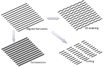 |
| This illustration depicts a new nano machine shop's ability to shape tiny wires, an advance that represents a possible future manufacturing method for applications ranging from high-speed electronics to solar cells. (Purdue University image/Gary Cheng) |
Abstract:
Laser Shock-Based Platform for Controllable Forming of Nanowires
Ji Li, Yiliang Liao, Sergey Suslov, and Gary J. Cheng*
Birck Nanotechnology Center and School of Industrial Engineering, Purdue University
One-dimensional nanomaterials have attracted a great deal of research interest in the past few decades due to their unique mechanical, electrical and optical properties. Changing the shape of nanowires (NWs) is both challenging and crucial to change the property and open wide functions of NWs, such as strain engineering, electronic transport, mechanical properties, band structure and quantum properties, etc. Here we report a scalable strategy to conduct cutting, bending and periodic straining of NWs by making use of laser shock pressure. Three-dimensional shaping of silver NWs is demonstrated, during which the Ag NWs exhibit very good ductility (strain-to-failure reaches 110%). Meanwhile, the high electrical conductivity of Ag NWs could retain well under controlled laser shock pressure. The microstructure observation indicates that the main deformation mechanism in Ag NWs under dynamic loading is formation of twinning and stacking fault, while dislocation motion and pile-up is less obvious. This method could be applied to semiconductor NWs as well.
'Nano machine shop' shapes nanowires, ultrathin films
West Lafayette, IN | Posted on August 29th, 2012A new "nano machine shop" that shapes nanowires and ultrathin films could represent a future manufacturing method for tiny structures with potentially revolutionary properties.
The structures might be tuned for applications ranging from high-speed electronics to solar cells and also may have greater strength and unusual traits such as ultrahigh magnetism and "plasmonic resonance," which could lead to improved optics, computers and electronics.
The researchers used their technique to stamp nano- and microgears; form tiny circular shapes out of a material called graphene, an ultrathin sheet of carbon that holds promise for advanced technologies; and change the shape of silver nanowires, said Gary Cheng, an associate professor of industrial engineering at Purdue University.
"We do this shaping at room temperature and atmospheric pressure, like a nano-machine shop," said Cheng, who is working with doctoral students Ji Li, Yiliang Liao, Ting-Fung Chung and Sergey Suslov and physics professor Yong P. Chen.
Graphene and nanowires - filaments 1,000 times thinner than a human hair - have numerous potential applications. However, technologies are needed to tailor them for specific uses. The new method, called laser shock-induced shaping, makes it possible to tune nanowires by altering electrical and optoelectrical properties that are critical for electronic components.
The researchers also have shown how laser shock-induced shaping can be used to change the properties of graphene, a step toward harnessing the material for electronic applications.
Findings were detailed in research papers published in the journal Nano Letters, and the work also was highlighted earlier this month in the News and Views section of the journal Nature Photonics. (The article is available at www.nature.com/nphoton/journal/v6/n8/full/nphoton.2012.186.html)
The technique works by using a multilayered sandwich structure that has a tiny mold at the bottom. Nanowires were situated directly above the mold, and other materials were layered between the nanowires and a glass cover sheet. Exposing this layered "forming unit" to an ultra-fast pulsing laser causes one of the layers to burn up, generating a downward pressure that forces the nanowires into the mold and changes their shape.
"The process could be scaled up for an industrial roll-to-roll manufacturing process by changing laser beam size and scanning speed," Cheng said. "The laser shock-induced shaping approach is fast and low-cost."
Part of the research, funded by the National Science Foundation, was carried out in a specialized clean room at the Birck Nanotechnology Center in Purdue's Discovery Park.
####
For more information, please click here
Contacts:
Writer:
Emil Venere
765-494-4709
Source:
Gary J. Cheng
765-494-5436
Copyright © Princeton University, Engineering School
If you have a comment, please Contact us.Issuers of news releases, not 7th Wave, Inc. or Nanotechnology Now, are solely responsible for the accuracy of the content.
Bookmark:


| Related News Press |
News and information
![]() Quantum computer improves AI predictions April 17th, 2026
Quantum computer improves AI predictions April 17th, 2026
![]() Flexible sensor gains sensitivity under pressure April 17th, 2026
Flexible sensor gains sensitivity under pressure April 17th, 2026
![]() A reusable chip for particulate matter sensing April 17th, 2026
A reusable chip for particulate matter sensing April 17th, 2026
![]() Detecting vibrational quantum beating in the predissociation dynamics of SF6 using time-resolved photoelectron spectroscopy April 17th, 2026
Detecting vibrational quantum beating in the predissociation dynamics of SF6 using time-resolved photoelectron spectroscopy April 17th, 2026
Thin films
![]() Tiny nanosheets, big leap: A new sensor detects ethanol at ultra-low levels January 30th, 2026
Tiny nanosheets, big leap: A new sensor detects ethanol at ultra-low levels January 30th, 2026
Graphene/ Graphite
![]() Electrifying results shed light on graphene foam as a potential material for lab grown cartilage June 6th, 2025
Electrifying results shed light on graphene foam as a potential material for lab grown cartilage June 6th, 2025
![]() Breakthrough in proton barrier films using pore-free graphene oxide: Kumamoto University researchers achieve new milestone in advanced coating technologies September 13th, 2024
Breakthrough in proton barrier films using pore-free graphene oxide: Kumamoto University researchers achieve new milestone in advanced coating technologies September 13th, 2024
NEMS
![]() IEDM - CEA-Leti Will Present 11 Papers and Host Workshop on Disruptive Technologies for Data Management November 7th, 2018
IEDM - CEA-Leti Will Present 11 Papers and Host Workshop on Disruptive Technologies for Data Management November 7th, 2018
![]() UT engineers develop first method for controlling nanomotors: Breakthrough for nanotechnology as UT engineers develop first method for switching the mechanical motion of nanomotors September 21st, 2018
UT engineers develop first method for controlling nanomotors: Breakthrough for nanotechnology as UT engineers develop first method for switching the mechanical motion of nanomotors September 21st, 2018
![]() Nano-kirigami: 'Paper-cut' provides model for 3D intelligent nanofabrication July 13th, 2018
Nano-kirigami: 'Paper-cut' provides model for 3D intelligent nanofabrication July 13th, 2018
![]() One string to rule them all April 17th, 2018
One string to rule them all April 17th, 2018
Govt.-Legislation/Regulation/Funding/Policy
![]() Quantum computer improves AI predictions April 17th, 2026
Quantum computer improves AI predictions April 17th, 2026
![]() Metasurfaces smooth light to boost magnetic sensing precision January 30th, 2026
Metasurfaces smooth light to boost magnetic sensing precision January 30th, 2026
![]() New imaging approach transforms study of bacterial biofilms August 8th, 2025
New imaging approach transforms study of bacterial biofilms August 8th, 2025
Nanoelectronics
![]() Lab to industry: InSe wafer-scale breakthrough for future electronics August 8th, 2025
Lab to industry: InSe wafer-scale breakthrough for future electronics August 8th, 2025
![]() Interdisciplinary: Rice team tackles the future of semiconductors Multiferroics could be the key to ultralow-energy computing October 6th, 2023
Interdisciplinary: Rice team tackles the future of semiconductors Multiferroics could be the key to ultralow-energy computing October 6th, 2023
![]() Key element for a scalable quantum computer: Physicists from Forschungszentrum J�lich and RWTH Aachen University demonstrate electron transport on a quantum chip September 23rd, 2022
Key element for a scalable quantum computer: Physicists from Forschungszentrum J�lich and RWTH Aachen University demonstrate electron transport on a quantum chip September 23rd, 2022
![]() Reduced power consumption in semiconductor devices September 23rd, 2022
Reduced power consumption in semiconductor devices September 23rd, 2022
Discoveries
![]() Quantum computer improves AI predictions April 17th, 2026
Quantum computer improves AI predictions April 17th, 2026
![]() Flexible sensor gains sensitivity under pressure April 17th, 2026
Flexible sensor gains sensitivity under pressure April 17th, 2026
![]() A reusable chip for particulate matter sensing April 17th, 2026
A reusable chip for particulate matter sensing April 17th, 2026
![]() Detecting vibrational quantum beating in the predissociation dynamics of SF6 using time-resolved photoelectron spectroscopy April 17th, 2026
Detecting vibrational quantum beating in the predissociation dynamics of SF6 using time-resolved photoelectron spectroscopy April 17th, 2026
Announcements
![]() A fundamentally new therapeutic approach to cystic fibrosis: Nanobody repairs cellular defect April 17th, 2026
A fundamentally new therapeutic approach to cystic fibrosis: Nanobody repairs cellular defect April 17th, 2026
![]() UC Irvine physicists discover method to reverse �quantum scrambling� : The work addresses the problem of information loss in quantum computing system April 17th, 2026
UC Irvine physicists discover method to reverse �quantum scrambling� : The work addresses the problem of information loss in quantum computing system April 17th, 2026
Energy
![]() Sensors innovations for smart lithium-based batteries: advancements, opportunities, and potential challenges August 8th, 2025
Sensors innovations for smart lithium-based batteries: advancements, opportunities, and potential challenges August 8th, 2025
![]() Simple algorithm paired with standard imaging tool could predict failure in lithium metal batteries August 8th, 2025
Simple algorithm paired with standard imaging tool could predict failure in lithium metal batteries August 8th, 2025
Photonics/Optics/Lasers
![]() Metasurfaces smooth light to boost magnetic sensing precision January 30th, 2026
Metasurfaces smooth light to boost magnetic sensing precision January 30th, 2026
![]() From sensors to smart systems: the rise of AI-driven photonic noses January 30th, 2026
From sensors to smart systems: the rise of AI-driven photonic noses January 30th, 2026
Solar/Photovoltaic
![]() Spinel-type sulfide semiconductors to operate the next-generation LEDs and solar cells For solar-cell absorbers and green-LED source October 3rd, 2025
Spinel-type sulfide semiconductors to operate the next-generation LEDs and solar cells For solar-cell absorbers and green-LED source October 3rd, 2025
![]() KAIST researchers introduce new and improved, next-generation perovskite solar cell November 8th, 2024
KAIST researchers introduce new and improved, next-generation perovskite solar cell November 8th, 2024
![]() Groundbreaking precision in single-molecule optoelectronics August 16th, 2024
Groundbreaking precision in single-molecule optoelectronics August 16th, 2024
![]() Development of zinc oxide nanopagoda array photoelectrode: photoelectrochemical water-splitting hydrogen production January 12th, 2024
Development of zinc oxide nanopagoda array photoelectrode: photoelectrochemical water-splitting hydrogen production January 12th, 2024
|
|
||
|
|
||
| The latest news from around the world, FREE | ||
|
|
||
|
|
||
| Premium Products | ||
|
|
||
|
Only the news you want to read!
Learn More |
||
|
|
||
|
Full-service, expert consulting
Learn More |
||
|
|
||