Home > Press > Powering the future: Smallest all-digital circuit opens doors to 5 nm next-gen semiconductor
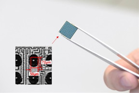 |
| Figure 1. Photograph of a chip containing the proposed PLL The entire all-digital PLL fits in a 50 × 72 μm2 region, making it the smallest PLL to date. |
Abstract:
Scientists at Tokyo Institute of Technology (Tokyo Tech) and Socionext Inc. have designed the world’s smallest all-digital phase-locked loop (PLL). PLLs are critical clocking circuits in virtually all digital applications, and reducing their size and improving their performance is a necessary step to enabling the development of next-generation technologies.
Powering the future: Smallest all-digital circuit opens doors to 5 nm next-gen semiconductor
Tokyo and Yokohama, Japan | Posted on February 11th, 2020New or improved technologies, such as artificial intelligence, 5G cellular communications, and the Internet-of-Things, are expected to bring revolutionary changes in society. But for that to happen, high-performance system-on-a-chip (SoC)—a type of integrated circuit—devices are indispensable. A core building block of SoC devices is the phase-locked loop (PLL), a circuit that synchronizes with the frequency of a reference oscillation and outputs a signal with the same or higher frequency. PLLs generate ‘clocking signals’, whose oscillations act as a metronome that provides a precise timing reference for the harmonious operation of digital devices.
For high performance SoC devices to be realized, fabrication processes for semiconductor electronics must become more sophisticated. The smaller the area to implement digital circuitry is, the better the performance of the device. Manufacturers have been racing to develop increasingly smaller semiconductors. 7 nm semiconductors (a massive improvement over their 10 nm predecessor) are already in production, and methods to build 5 nm ones are now being looked at.
However, in this endeavor stands a major bottleneck. Existing PLLs require analog components, which are generally bulky and have designs that are difficult to scale down.
Scientists at Tokyo Tech and Socionext Inc., led by Prof. Kenichi Okada, have addressed this issue by implementing a ‘synthesizable’ fractional-N PLL, which only requires digital logic gates, and no bulky analog components, making it easy to adopt in conventional miniaturized integrated circuits.
Okada and team used several techniques to decrease the required area, power consumption and jitter—unwanted time fluctuations when transmitting digital signals—of their synthesizable PLLs. To decrease area, they employed a ring oscillator, a compact oscillator that can be easily scaled down. To suppress jitter, they reduced the phase noise—random fluctuations in a signal—of this ring oscillator, using ‘injection locking’—the process of synchronizing an oscillator with an external signal whose frequency (or multiple of it) is close to that of the oscillator—over a wide range of frequencies. The lower phase noise, in turn, reduced power consumption.
The design of this synthesizable PLL beats that of all other current state-of-the-art PLLs in many important aspects. It achieves the best jitter performance with the lowest power consumption and smallest area (as can be seen in Figure 1). “The core area is 0.0036 mm2, and the whole PLL is implemented as one layout with a single power supply,” remarks Okada. Further, it can be built using standard digital design tools, allowing for its rapid, low-effort, and low-cost production, making it commercially viable.
This synthesizable PLL can be easily integrated into the design of all-digital SoCs, and is commercially viable, making it valuable for developing the much sought after 5 nm semiconductor for cutting-edge applications including artificial intelligence, internet of things and many others, where high performance and low power consumption would be the critical requirements. But the contributions of this research go beyond these possibilities. “Our work demonstrates the potential of synthesizable circuits. With the design methodology employed here, other building blocks of SoCs, such as data converters, power management circuits, and wireless transceivers, could be made synthesizable as well. This would greatly boost design productivity and considerably reduce design efforts,” explains Okada. Tokyo Tech and Socionext will continue their collaboration in this filed to advance the miniaturization of electronic devices, enabling the realization of newer-generation technologies.
This research work was conducted in cooperation with TeraPixel Technologies Inc.
Affiliations:
[1] Tokyo Institute of Technology, Tokyo, Japan [
[2] Socionext Inc., Yokohama, Japan
*Corresponding author’s email:
####
About Tokyo Institute of Technology
Tokyo Tech stands at the forefront of research and higher education as the leading university for science and technology in Japan. Tokyo Tech researchers excel in fields ranging from materials science to biology, computer science, and physics. Founded in 1881, Tokyo Tech hosts over 10,000 undergraduate and graduate students per year, who develop into scientific leaders and some of the most sought-after engineers in industry. Embodying the Japanese philosophy of “monotsukuri,” meaning “technical ingenuity and innovation,” the Tokyo Tech community strives to contribute to society through high-impact research.
www.titech.ac.jp/english/
About Socionext
Socionext is a global, innovative enterprise that designs, develops and delivers System-on-Chip solutions to customers worldwide. The company is focused on technologies that drive today’s leading-edge applications in consumer, automotive and industrial markets. Socionext combines world-class expertise, experience, and an extensive IP portfolio to provide exceptional solutions and ensure a better quality of experience for customers. Founded in 2015, Socionext Inc. is headquartered in Yokohama, and has offices in Japan, Asia, United States and Europe to lead its product development and sales activities. For more information, visit www.socionext.com.
For more information, please click here
Contacts:
Emiko Kawaguchi
Public Relations Section,
Tokyo Institute of Technology
+81-3-5734-2975
Corporate Planning Office
Socionext Inc.
http://www.socionext.com/en/contact
+81-45-568-1006
Copyright © Tokyo Institute of Technology
If you have a comment, please Contact us.Issuers of news releases, not 7th Wave, Inc. or Nanotechnology Now, are solely responsible for the accuracy of the content.
Bookmark:


| Related Links |
| Related News Press |
News and information
![]() Quantum computer improves AI predictions April 17th, 2026
Quantum computer improves AI predictions April 17th, 2026
![]() Flexible sensor gains sensitivity under pressure April 17th, 2026
Flexible sensor gains sensitivity under pressure April 17th, 2026
![]() A reusable chip for particulate matter sensing April 17th, 2026
A reusable chip for particulate matter sensing April 17th, 2026
![]() Detecting vibrational quantum beating in the predissociation dynamics of SF6 using time-resolved photoelectron spectroscopy April 17th, 2026
Detecting vibrational quantum beating in the predissociation dynamics of SF6 using time-resolved photoelectron spectroscopy April 17th, 2026
Wireless/telecommunications/RF/Antennas/Microwaves
![]() Researchers develop molecular qubits that communicate at telecom frequencies October 3rd, 2025
Researchers develop molecular qubits that communicate at telecom frequencies October 3rd, 2025
![]() HKUST researchers develop new integration technique for efficient coupling of III-V and silicon February 16th, 2024
HKUST researchers develop new integration technique for efficient coupling of III-V and silicon February 16th, 2024
![]() Researchers demonstrate co-propagation of quantum and classical signals: Study shows that quantum encryption can be implemented in existing fiber networks January 20th, 2023
Researchers demonstrate co-propagation of quantum and classical signals: Study shows that quantum encryption can be implemented in existing fiber networks January 20th, 2023
Internet-of-Things
![]() Nanofibrous metal oxide semiconductor for sensory face November 8th, 2024
Nanofibrous metal oxide semiconductor for sensory face November 8th, 2024
![]() New nanowire sensors are the next step in the Internet of Things January 6th, 2023
New nanowire sensors are the next step in the Internet of Things January 6th, 2023
Hardware
![]() The present and future of computing get a boost from new research July 21st, 2023
The present and future of computing get a boost from new research July 21st, 2023
Possible Futures
![]() A fundamentally new therapeutic approach to cystic fibrosis: Nanobody repairs cellular defect April 17th, 2026
A fundamentally new therapeutic approach to cystic fibrosis: Nanobody repairs cellular defect April 17th, 2026
![]() UC Irvine physicists discover method to reverse ‘quantum scrambling’ : The work addresses the problem of information loss in quantum computing system April 17th, 2026
UC Irvine physicists discover method to reverse ‘quantum scrambling’ : The work addresses the problem of information loss in quantum computing system April 17th, 2026
Chip Technology
![]() A reusable chip for particulate matter sensing April 17th, 2026
A reusable chip for particulate matter sensing April 17th, 2026
![]() Metasurfaces smooth light to boost magnetic sensing precision January 30th, 2026
Metasurfaces smooth light to boost magnetic sensing precision January 30th, 2026
Nanoelectronics
![]() Lab to industry: InSe wafer-scale breakthrough for future electronics August 8th, 2025
Lab to industry: InSe wafer-scale breakthrough for future electronics August 8th, 2025
![]() Interdisciplinary: Rice team tackles the future of semiconductors Multiferroics could be the key to ultralow-energy computing October 6th, 2023
Interdisciplinary: Rice team tackles the future of semiconductors Multiferroics could be the key to ultralow-energy computing October 6th, 2023
![]() Key element for a scalable quantum computer: Physicists from Forschungszentrum Jülich and RWTH Aachen University demonstrate electron transport on a quantum chip September 23rd, 2022
Key element for a scalable quantum computer: Physicists from Forschungszentrum Jülich and RWTH Aachen University demonstrate electron transport on a quantum chip September 23rd, 2022
![]() Reduced power consumption in semiconductor devices September 23rd, 2022
Reduced power consumption in semiconductor devices September 23rd, 2022
Discoveries
![]() Quantum computer improves AI predictions April 17th, 2026
Quantum computer improves AI predictions April 17th, 2026
![]() Flexible sensor gains sensitivity under pressure April 17th, 2026
Flexible sensor gains sensitivity under pressure April 17th, 2026
![]() A reusable chip for particulate matter sensing April 17th, 2026
A reusable chip for particulate matter sensing April 17th, 2026
![]() Detecting vibrational quantum beating in the predissociation dynamics of SF6 using time-resolved photoelectron spectroscopy April 17th, 2026
Detecting vibrational quantum beating in the predissociation dynamics of SF6 using time-resolved photoelectron spectroscopy April 17th, 2026
Announcements
![]() A fundamentally new therapeutic approach to cystic fibrosis: Nanobody repairs cellular defect April 17th, 2026
A fundamentally new therapeutic approach to cystic fibrosis: Nanobody repairs cellular defect April 17th, 2026
![]() UC Irvine physicists discover method to reverse ‘quantum scrambling’ : The work addresses the problem of information loss in quantum computing system April 17th, 2026
UC Irvine physicists discover method to reverse ‘quantum scrambling’ : The work addresses the problem of information loss in quantum computing system April 17th, 2026
Interviews/Book Reviews/Essays/Reports/Podcasts/Journals/White papers/Posters
![]() A fundamentally new therapeutic approach to cystic fibrosis: Nanobody repairs cellular defect April 17th, 2026
A fundamentally new therapeutic approach to cystic fibrosis: Nanobody repairs cellular defect April 17th, 2026
![]() UC Irvine physicists discover method to reverse ‘quantum scrambling’ : The work addresses the problem of information loss in quantum computing system April 17th, 2026
UC Irvine physicists discover method to reverse ‘quantum scrambling’ : The work addresses the problem of information loss in quantum computing system April 17th, 2026
Artificial Intelligence
![]() Quantum computer improves AI predictions April 17th, 2026
Quantum computer improves AI predictions April 17th, 2026
![]() From sensors to smart systems: the rise of AI-driven photonic noses January 30th, 2026
From sensors to smart systems: the rise of AI-driven photonic noses January 30th, 2026
![]() New quantum encoding methods slash circuit complexity in machine learning November 8th, 2024
New quantum encoding methods slash circuit complexity in machine learning November 8th, 2024
|
|
||
|
|
||
| The latest news from around the world, FREE | ||
|
|
||
|
|
||
| Premium Products | ||
|
|
||
|
Only the news you want to read!
Learn More |
||
|
|
||
|
Full-service, expert consulting
Learn More |
||
|
|
||