Home > Press > Designer electronics out of the printer: Optimized printing process enables custom organic electronics
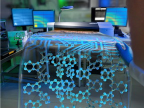 |
| Organic electronics, based on conducting polymers, are hailed as a promising future market. This is the cover illustration of Advanced Materials (10.1002/adma.201570148). CREDIT: Artwork: Christoph Hohmann / Nanosystems Initiative Munich |
Abstract:
They are thin, light-weight, flexible and can be produced cost- and energy-efficiently: printed microelectronic components made of synthetics. Flexible displays and touch screens, glowing films, RFID tags and solar cells represent a future market. In the context of an international cooperation project, physicists at the Technische Universität München (TUM) have now observed the creation of razor thin polymer electrodes during the printing process and successfully improved the electrical properties of the printed films.
Designer electronics out of the printer: Optimized printing process enables custom organic electronics
Muenchen, Germany | Posted on June 16th, 2015Solar cells out of a printer? This seemed unthinkable only a few years ago. There were hardly any alternatives to classical silicon technology available. In the mean time touch screens, sensors and solar cells can be made of conducting polymers. Flexible monitors and glowing wall paper made of organic light emitting diodes, so-called OLEDs, are in rapid development. The "organic electronics" are hailed as a promising future market.
However, the technology also has its pitfalls: To manufacture the components on an industrial scale, semiconducting or insulating layers - each a thousand times thinner than a human hair - must be printed onto a carrier film in a predefined order. "This is a highly complex process, whose details need to be fully understood to allow custom-tailored applications," explains Professor Peter Müller-Buschbaum of the Chair of Functional Materials at TU München.
A further challenge is the contacting between flexible, conducting layers. Hitherto electronic contacts made of crystalline indium tin oxide were frequently used. However, this construction has numerous drawbacks: The oxide is more brittle than the polymer layers over them, which limits the flexibility of the cells. Furthermore, the manufacturing process also consumes much energy. Finally, indium is a rare element that exists only in very limited quantities.
Polymers in X-ray light
A few months ago, researchers from the Lawrence Berkeley National Laboratory in California for the first time succeeded in observing the cross-linking of polymer molecules in the active layer of an organic solar cell during the printing process. In collaboration with their colleagues in California, Müller-Buschbaum's team took advantage of this technology to improve the characteristics of the polymer electronic elements.
The researchers used X-ray radiation generated in the Berkley synchrotron for their investigations. The X-rays are directed to the freshly printed synthetic layer and scattered. The arrangement and orientation of the molecules during the curing process of the printed films can be determined from changes in the scattering pattern.
"Thanks to the very intensive X-ray radiation we can achieve a very high time resolution," says Claudia M. Palumbiny. In Berkeley the physicist from the TUM investigated the "blocking layer" that sorts and selectively transports the charge carriers in the organic electronic components. The TUM research team is now, together with its US colleagues, publishing the results in the trade journal Advanced Materials.
Custom properties
"In our work, we showed for the first time ever that even small changes in the physico-chemical process conditions have a significant influence on the build-up and properties of the layer," says Claudia M. Palumbiny. "Adding solvents with a high boiling point, for example, improves segregation in synthetics components. This improves the crystallization in conducting molecules. The distance between the molecules shrinks and the conductivity increases.
In this manner stability and conductivity can be improved to such an extent that the material can be deployed not only as a blocking layer, but even as a transparent, electrical contact. This can be used to replace the brittle indium tin oxide layers. "At the end of the day, this means that all layers could be produced using the same process," explains Palumbiny. "That would be a great advantage for manufacturers."
To make all of this possible one day, TUM researchers want to continue investigating and optimizing the electrode material further and make their know-how available to industry. "We have now formed the basis for pushing ahead materials development with future investigations so that these can be taken over by industrial enterprises," explains Prof. Müller-Buschbaum.
###
The research was supported by the GreenTech Initiative "Interface Science for Photovoltaics" (ISPV) of the EuroTech Universities together with the International Graduate School of Science and Engineering (IGSSE) at TUM and by the Cluster of Excellence "Nanosystems Initiative Munich" (NIM). Further support came from the Elite Network of Bavaria's International Doctorate Program "NanoBioTechnology" (IDK-NBT) and the Center for NanoScience (CeNS) and from "Polymer-Based Materials for Harvesting Solar Energy" (PHaSE), an Energy Frontier Research Center funded by the U.S. Department of Energy, Office of Basic Energy Sciences. Portions of the research were carried out at the Advanced Light Source which receives support by the Office of Basic Energy Sciences of the U.S. Department of Energy.
Publication:
The Crystallization of PEDOT:PSS Polymeric Electrodes Probed In Situ during Printing
Claudia M. Palumbiny, Feng Liu, Thomas P. Russell, Alexander Hexemer, Cheng Wang, and Peter Müller-Buschbaum
Advanced Materials, June 10, 2015, 27, 22, 3391-3397 - DOI: 10.1002/adma.201500315
####
For more information, please click here
Contacts:
Dr. Andreas Battenberg
49-892-891-0510
Copyright © Technische Universitaet Muenchen
If you have a comment, please Contact us.Issuers of news releases, not 7th Wave, Inc. or Nanotechnology Now, are solely responsible for the accuracy of the content.
Bookmark:


| Related News Press |
News and information
![]() Quantum computer improves AI predictions April 17th, 2026
Quantum computer improves AI predictions April 17th, 2026
![]() Flexible sensor gains sensitivity under pressure April 17th, 2026
Flexible sensor gains sensitivity under pressure April 17th, 2026
![]() A reusable chip for particulate matter sensing April 17th, 2026
A reusable chip for particulate matter sensing April 17th, 2026
![]() Detecting vibrational quantum beating in the predissociation dynamics of SF6 using time-resolved photoelectron spectroscopy April 17th, 2026
Detecting vibrational quantum beating in the predissociation dynamics of SF6 using time-resolved photoelectron spectroscopy April 17th, 2026
Display technology/LEDs/SS Lighting/OLEDs
![]() Spinel-type sulfide semiconductors to operate the next-generation LEDs and solar cells For solar-cell absorbers and green-LED source October 3rd, 2025
Spinel-type sulfide semiconductors to operate the next-generation LEDs and solar cells For solar-cell absorbers and green-LED source October 3rd, 2025
![]() Efficient and stable hybrid perovskite-organic light-emitting diodes with external quantum efficiency exceeding 40 per cent July 5th, 2024
Efficient and stable hybrid perovskite-organic light-emitting diodes with external quantum efficiency exceeding 40 per cent July 5th, 2024
Govt.-Legislation/Regulation/Funding/Policy
![]() Quantum computer improves AI predictions April 17th, 2026
Quantum computer improves AI predictions April 17th, 2026
![]() Metasurfaces smooth light to boost magnetic sensing precision January 30th, 2026
Metasurfaces smooth light to boost magnetic sensing precision January 30th, 2026
![]() New imaging approach transforms study of bacterial biofilms August 8th, 2025
New imaging approach transforms study of bacterial biofilms August 8th, 2025
Sensors
![]() Flexible sensor gains sensitivity under pressure April 17th, 2026
Flexible sensor gains sensitivity under pressure April 17th, 2026
![]() Tiny nanosheets, big leap: A new sensor detects ethanol at ultra-low levels January 30th, 2026
Tiny nanosheets, big leap: A new sensor detects ethanol at ultra-low levels January 30th, 2026
![]() From sensors to smart systems: the rise of AI-driven photonic noses January 30th, 2026
From sensors to smart systems: the rise of AI-driven photonic noses January 30th, 2026
![]() Sensors innovations for smart lithium-based batteries: advancements, opportunities, and potential challenges August 8th, 2025
Sensors innovations for smart lithium-based batteries: advancements, opportunities, and potential challenges August 8th, 2025
Discoveries
![]() Quantum computer improves AI predictions April 17th, 2026
Quantum computer improves AI predictions April 17th, 2026
![]() Flexible sensor gains sensitivity under pressure April 17th, 2026
Flexible sensor gains sensitivity under pressure April 17th, 2026
![]() A reusable chip for particulate matter sensing April 17th, 2026
A reusable chip for particulate matter sensing April 17th, 2026
![]() Detecting vibrational quantum beating in the predissociation dynamics of SF6 using time-resolved photoelectron spectroscopy April 17th, 2026
Detecting vibrational quantum beating in the predissociation dynamics of SF6 using time-resolved photoelectron spectroscopy April 17th, 2026
Materials/Metamaterials/Magnetoresistance
![]() First real-time observation of two-dimensional melting process: Researchers at Mainz University unveil new insights into magnetic vortex structures August 8th, 2025
First real-time observation of two-dimensional melting process: Researchers at Mainz University unveil new insights into magnetic vortex structures August 8th, 2025
![]() Researchers unveil a groundbreaking clay-based solution to capture carbon dioxide and combat climate change June 6th, 2025
Researchers unveil a groundbreaking clay-based solution to capture carbon dioxide and combat climate change June 6th, 2025
![]() A 1960s idea inspires NBI researchers to study hitherto inaccessible quantum states June 6th, 2025
A 1960s idea inspires NBI researchers to study hitherto inaccessible quantum states June 6th, 2025
![]() Institute for Nanoscience hosts annual proposal planning meeting May 16th, 2025
Institute for Nanoscience hosts annual proposal planning meeting May 16th, 2025
Announcements
![]() A fundamentally new therapeutic approach to cystic fibrosis: Nanobody repairs cellular defect April 17th, 2026
A fundamentally new therapeutic approach to cystic fibrosis: Nanobody repairs cellular defect April 17th, 2026
![]() UC Irvine physicists discover method to reverse ‘quantum scrambling’ : The work addresses the problem of information loss in quantum computing system April 17th, 2026
UC Irvine physicists discover method to reverse ‘quantum scrambling’ : The work addresses the problem of information loss in quantum computing system April 17th, 2026
Interviews/Book Reviews/Essays/Reports/Podcasts/Journals/White papers/Posters
![]() A fundamentally new therapeutic approach to cystic fibrosis: Nanobody repairs cellular defect April 17th, 2026
A fundamentally new therapeutic approach to cystic fibrosis: Nanobody repairs cellular defect April 17th, 2026
![]() UC Irvine physicists discover method to reverse ‘quantum scrambling’ : The work addresses the problem of information loss in quantum computing system April 17th, 2026
UC Irvine physicists discover method to reverse ‘quantum scrambling’ : The work addresses the problem of information loss in quantum computing system April 17th, 2026
Energy
![]() Sensors innovations for smart lithium-based batteries: advancements, opportunities, and potential challenges August 8th, 2025
Sensors innovations for smart lithium-based batteries: advancements, opportunities, and potential challenges August 8th, 2025
![]() Simple algorithm paired with standard imaging tool could predict failure in lithium metal batteries August 8th, 2025
Simple algorithm paired with standard imaging tool could predict failure in lithium metal batteries August 8th, 2025
Research partnerships
![]() Lab to industry: InSe wafer-scale breakthrough for future electronics August 8th, 2025
Lab to industry: InSe wafer-scale breakthrough for future electronics August 8th, 2025
![]() HKU physicists uncover hidden order in the quantum world through deconfined quantum critical points April 25th, 2025
HKU physicists uncover hidden order in the quantum world through deconfined quantum critical points April 25th, 2025
Solar/Photovoltaic
![]() Spinel-type sulfide semiconductors to operate the next-generation LEDs and solar cells For solar-cell absorbers and green-LED source October 3rd, 2025
Spinel-type sulfide semiconductors to operate the next-generation LEDs and solar cells For solar-cell absorbers and green-LED source October 3rd, 2025
![]() KAIST researchers introduce new and improved, next-generation perovskite solar cell November 8th, 2024
KAIST researchers introduce new and improved, next-generation perovskite solar cell November 8th, 2024
![]() Groundbreaking precision in single-molecule optoelectronics August 16th, 2024
Groundbreaking precision in single-molecule optoelectronics August 16th, 2024
![]() Development of zinc oxide nanopagoda array photoelectrode: photoelectrochemical water-splitting hydrogen production January 12th, 2024
Development of zinc oxide nanopagoda array photoelectrode: photoelectrochemical water-splitting hydrogen production January 12th, 2024
RFID
![]() Nanowire 'inks' enable paper-based printable electronics: Highly conductive films make functional circuits without adding high heat January 4th, 2017
Nanowire 'inks' enable paper-based printable electronics: Highly conductive films make functional circuits without adding high heat January 4th, 2017
![]() Conformal transfer of graphene for reproducible device fabrication August 11th, 2015
Conformal transfer of graphene for reproducible device fabrication August 11th, 2015
Printing/Lithography/Inkjet/Inks/Bio-printing/Dyes
![]() Presenting: Ultrasound-based printing of 3D materials—potentially inside the body December 8th, 2023
Presenting: Ultrasound-based printing of 3D materials—potentially inside the body December 8th, 2023
![]() Simple ballpoint pen can write custom LEDs August 11th, 2023
Simple ballpoint pen can write custom LEDs August 11th, 2023
![]() Disposable electronics on a simple sheet of paper October 7th, 2022
Disposable electronics on a simple sheet of paper October 7th, 2022
|
|
||
|
|
||
| The latest news from around the world, FREE | ||
|
|
||
|
|
||
| Premium Products | ||
|
|
||
|
Only the news you want to read!
Learn More |
||
|
|
||
|
Full-service, expert consulting
Learn More |
||
|
|
||