Home > Press > Conformal transfer of graphene for reproducible device fabrication
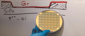 |
| Reliable wafer scale production of graphene devices. |
Abstract:
Conformal transfer of graphene on a prepatterned substrate is a viable technology for reproducible fabrication of graphene devices. Such is the conclusion of a recent study by a team of scientists from Germany, the Netherlands, Spain and Saudi Arabia.
Conformal transfer of graphene for reproducible device fabrication
San Sebastian, Spain | Posted on August 11th, 2015Reliable fabrication of graphene devices for electronics has been a technological challenge for the graphene community for years. Large area high quality graphene, required for high-tech applications, is typically grown by chemical vapor deposition (CVD) on metal foils. Following growth, the graphene film is transferred to an electronically useful substrate, which is commonly SiO2 on Si. Standard procedure follows these steps up with photolithographic patterning of devices and evaporation of gold contacts.
In the past, this sequence of steps failed to result in devices of consistently high quality, as each fabrication step introduced unpredictable defects. The film growth was the first step to be perfected by a global network of busy scientists. Graphene transfer was in parallel mastered by the Spanish company Graphenea, a participant of this most recent breakthrough, as evidenced by their patent award earlier this year. Still, lithography and evaporation would cause film breaks, cracks and wrinkles, which were unpredictable and which lowered the quality of the final devices. Now, researchers have turned the fabrication upside down by performing lithography and contact evaporation prior to graphene transfer. The result is a reliable method for wafer-scale fabrication of graphene devices.
The paper, recently published in Applied Materials & Interfaces (a publication of the American Chemical Society), starts by considering the values reported in literature for contact and sheet resistance obtained with the standard graphene fabrication and transfer method. Focusing on graphene grown by CVD, the researchers find that there is significant scatter in the reported values, spanning nearly an order of magnitude. The scientists then performed the standard procedure themselves, finding that the resulting graphene sheet is inhomogeneous, with defects appearing in random places.
Following the improved process, in which the contact patterning and metal deposition are performed prior to the transfer, yields a much better result. The graphene sheet is smooth and uniform across the wafer, conformally covering the electrode structures. Electrical measurements indicate good device reproducibility, with sheet resistance low enough to consider using these graphene devices in radio frequency electronics. The potential application of the graphene channels is additionally confirmed by steady device performance over a wide range of applied current, up to 0.5 A. The careful fabrication led to devices that support the highest current density ever reported in transferred CVD graphene.
Over 600 devices were tested, showing a very narrow spread in the measured parameters. Such statistical similarity not only opens a gate to mass production of graphene devices for radio frequency applications, but immediately allows the testing of fundamental device physics of monolayer materials.
####
For more information, please click here
Contacts:
Headquarters
Graphenea
Avenida de Tolosa, 76
20018 - Donostia/San Sebasti�n
Spain
Copyright © Graphenea Inc.
If you have a comment, please Contact us.Issuers of news releases, not 7th Wave, Inc. or Nanotechnology Now, are solely responsible for the accuracy of the content.
Bookmark:


| Related News Press |
Graphene/ Graphite
![]() Electrifying results shed light on graphene foam as a potential material for lab grown cartilage June 6th, 2025
Electrifying results shed light on graphene foam as a potential material for lab grown cartilage June 6th, 2025
![]() Breakthrough in proton barrier films using pore-free graphene oxide: Kumamoto University researchers achieve new milestone in advanced coating technologies September 13th, 2024
Breakthrough in proton barrier films using pore-free graphene oxide: Kumamoto University researchers achieve new milestone in advanced coating technologies September 13th, 2024
Chip Technology
![]() A reusable chip for particulate matter sensing April 17th, 2026
A reusable chip for particulate matter sensing April 17th, 2026
![]() Metasurfaces smooth light to boost magnetic sensing precision January 30th, 2026
Metasurfaces smooth light to boost magnetic sensing precision January 30th, 2026
Discoveries
![]() Quantum computer improves AI predictions April 17th, 2026
Quantum computer improves AI predictions April 17th, 2026
![]() Flexible sensor gains sensitivity under pressure April 17th, 2026
Flexible sensor gains sensitivity under pressure April 17th, 2026
![]() A reusable chip for particulate matter sensing April 17th, 2026
A reusable chip for particulate matter sensing April 17th, 2026
![]() Detecting vibrational quantum beating in the predissociation dynamics of SF6 using time-resolved photoelectron spectroscopy April 17th, 2026
Detecting vibrational quantum beating in the predissociation dynamics of SF6 using time-resolved photoelectron spectroscopy April 17th, 2026
Materials/Metamaterials/Magnetoresistance
![]() First real-time observation of two-dimensional melting process: Researchers at Mainz University unveil new insights into magnetic vortex structures August 8th, 2025
First real-time observation of two-dimensional melting process: Researchers at Mainz University unveil new insights into magnetic vortex structures August 8th, 2025
![]() Researchers unveil a groundbreaking clay-based solution to capture carbon dioxide and combat climate change June 6th, 2025
Researchers unveil a groundbreaking clay-based solution to capture carbon dioxide and combat climate change June 6th, 2025
![]() A 1960s idea inspires NBI researchers to study hitherto inaccessible quantum states June 6th, 2025
A 1960s idea inspires NBI researchers to study hitherto inaccessible quantum states June 6th, 2025
![]() Institute for Nanoscience hosts annual proposal planning meeting May 16th, 2025
Institute for Nanoscience hosts annual proposal planning meeting May 16th, 2025
Announcements
![]() A fundamentally new therapeutic approach to cystic fibrosis: Nanobody repairs cellular defect April 17th, 2026
A fundamentally new therapeutic approach to cystic fibrosis: Nanobody repairs cellular defect April 17th, 2026
![]() UC Irvine physicists discover method to reverse �quantum scrambling� : The work addresses the problem of information loss in quantum computing system April 17th, 2026
UC Irvine physicists discover method to reverse �quantum scrambling� : The work addresses the problem of information loss in quantum computing system April 17th, 2026
Interviews/Book Reviews/Essays/Reports/Podcasts/Journals/White papers/Posters
![]() A fundamentally new therapeutic approach to cystic fibrosis: Nanobody repairs cellular defect April 17th, 2026
A fundamentally new therapeutic approach to cystic fibrosis: Nanobody repairs cellular defect April 17th, 2026
![]() UC Irvine physicists discover method to reverse �quantum scrambling� : The work addresses the problem of information loss in quantum computing system April 17th, 2026
UC Irvine physicists discover method to reverse �quantum scrambling� : The work addresses the problem of information loss in quantum computing system April 17th, 2026
Patents/IP/Tech Transfer/Licensing
![]() Getting drugs across the blood-brain barrier using nanoparticles March 3rd, 2023
Getting drugs across the blood-brain barrier using nanoparticles March 3rd, 2023
![]() Metasurfaces control polarized light at will: New research unlocks the hidden potential of metasurfaces August 13th, 2021
Metasurfaces control polarized light at will: New research unlocks the hidden potential of metasurfaces August 13th, 2021
![]() Arrowhead Pharmaceuticals Announces Closing of Agreement with Takeda November 27th, 2020
Arrowhead Pharmaceuticals Announces Closing of Agreement with Takeda November 27th, 2020
Research partnerships
![]() Lab to industry: InSe wafer-scale breakthrough for future electronics August 8th, 2025
Lab to industry: InSe wafer-scale breakthrough for future electronics August 8th, 2025
![]() HKU physicists uncover hidden order in the quantum world through deconfined quantum critical points April 25th, 2025
HKU physicists uncover hidden order in the quantum world through deconfined quantum critical points April 25th, 2025
New-Contracts/Sales/Customers
![]() Bruker Light-Sheet Microscopes at Major Comprehensive Cancer Center: New Advanced Imaging Center Powered by Two MuVi and LCS SPIM Microscopes March 25th, 2021
Bruker Light-Sheet Microscopes at Major Comprehensive Cancer Center: New Advanced Imaging Center Powered by Two MuVi and LCS SPIM Microscopes March 25th, 2021
![]() Arrowhead Pharmaceuticals Announces Closing of Agreement with Takeda November 27th, 2020
Arrowhead Pharmaceuticals Announces Closing of Agreement with Takeda November 27th, 2020
![]() Veeco Announces Aledia Order of 300mm MOCVD Equipment for microLED Displays: Propel� Platform First 300mm System with EFEM Designed for Advanced Display Applications October 20th, 2020
Veeco Announces Aledia Order of 300mm MOCVD Equipment for microLED Displays: Propel� Platform First 300mm System with EFEM Designed for Advanced Display Applications October 20th, 2020
![]() GREENWAVES TECHNOLOGIES Announces Next Generation GAP9 Hearables Platform Using GLOBALFOUNDRIES 22FDX Solution October 16th, 2020
GREENWAVES TECHNOLOGIES Announces Next Generation GAP9 Hearables Platform Using GLOBALFOUNDRIES 22FDX Solution October 16th, 2020
RFID
![]() Nanowire 'inks' enable paper-based printable electronics: Highly conductive films make functional circuits without adding high heat January 4th, 2017
Nanowire 'inks' enable paper-based printable electronics: Highly conductive films make functional circuits without adding high heat January 4th, 2017
![]() Designer electronics out of the printer: Optimized printing process enables custom organic electronics June 16th, 2015
Designer electronics out of the printer: Optimized printing process enables custom organic electronics June 16th, 2015
|
|
||
|
|
||
| The latest news from around the world, FREE | ||
|
|
||
|
|
||
| Premium Products | ||
|
|
||
|
Only the news you want to read!
Learn More |
||
|
|
||
|
Full-service, expert consulting
Learn More |
||
|
|
||