Home > Press > NRL discovers two-dimensional waveguides
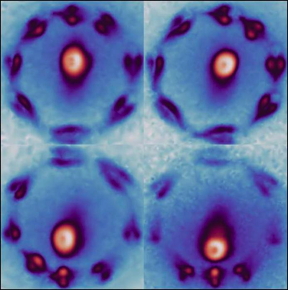 |
| Confocal microscope image of waveguided photoluminescence in a hexagonal boron nitride waveguide. The lobe-pattern around the edges is reminiscent of koi circling a pond. Image taken by Samuel LaGasse in April 2023. CREDIT U.S. Naval Research Laboratory/Samuel LaGasse |
Abstract:
The U.S. Naval Research Laboratory (NRL), in collaboration with Kansas State University, announce the discovery of slab waveguides based on the two-dimensional material hexagonal boron nitride. This milestone has been reported in the journal Advanced Materials.
NRL discovers two-dimensional waveguides
Washington, DC | Posted on February 16th, 2024Two-dimensional (2D) materials are a class of materials which can be reduced to the monolayer limit by mechanically peeling the layers apart. The weak interlayer attractions, or van der Waals attraction, allows the layers to be separated via the so-called �Scotch tape� method. The most famous 2D material, graphene, is a semimetallic material consisting of a single layer of carbon atoms. Recently, other 2D materials including semiconducting transition metal dichalcogenides (TMDs) and insulating hexagonal boron nitride (hBN) have also garnered attention. When reduced near the monolayer limit, 2D materials have unique nanoscale properties which are appealing for creating atomically thin electronic and optical devices.
�We knew using hexagonal boron nitride would lead to outstanding optical properties in our samples, none of us expected that it would also act a waveguide,� said Samuel Lagasse, Ph.D., Novel Materials and Applications Division. �Since hBN is used so widely in 2D material�based devices, this novel usage as an optical waveguide potentially has wide-ranging impacts.�
Graphene and TMD monolayers are both extremely sensitive to the surrounding environment. Therefore, researchers have sought to protect these materials by encapsulating them in a passivating layer. This is where hBN comes in: layers of hBN are able to �screen� impurities near graphene or TMD layers, leading to fantastic properties. In recent NRL-led work, the thickness of hBN surrounding a light-emitting TMD layer was carefully tuned in order to support optical waveguide modes.
Researchers at NRL carefully assembled stacks of 2D materials, known as �van der Waals heterostructures.� These heterostructures can have specialized properties due to the layering. Slabs of hBN were placed around single layers of TMDs, such as molybdenum diselenide or tungsten diselenide, which can emit light in the visible and near-infrared. The slabs of hBN were carefully tuned in thickness so that the emitted light would be trapped within the hBN and waveguided. When the light waveguides to the edge of the hBN, it can scatter out and be detected by a microscope.
The research was motivated by the challenges of optical measurements of 2D TMDs. When laser light is focused on TMDs, particles known as excitons are generated. Most excitons emit light out of the plane of the TMD, however an elusive type of exciton known as a �dark� exciton exists in some TMDs, emits in the plane of the TMD. NRL�s slab waveguides capture the light from the dark excitons, providing a way to study them optically.
�2D materials have exotic optoelectronic properties that will be useful to the Navy,� said Lagasse. �A large challenge is interfacing these materials with existing platforms without damaging them � these boron nitride waveguides are a step towards that realization.�
NRL researchers used two special types of optical microscopes to characterize the hBN waveguides. One setup allows researchers to spectroscopically resolve photoluminescence emitting from different spots of the waveguide. The other setup let them observe the angular distribution of the emitted light.
NRL researchers also developed 3D electromagnetic models of the waveguides. The modeling results provide a toolkit for designing future 2D devices that use slab waveguides.
####
About U.S. Naval Research Laboratory
L is a scientific and engineering command dedicated to research that drives innovative advances for the U.S. Navy and Marine Corps from the seafloor to space and in the information domain. NRL is located in Washington, D.C. with major field sites in Stennis Space Center, Mississippi; Key West, Florida; Monterey, California, and employs approximately 3,000 civilian scientists, engineers and support personnel.
For more information, contact NRL Corporate Communications at (202) 480-3746 or .
For more information, please click here
Contacts:
Mary Hamisevicz
U.S. Naval Research Laboratory
Cell: (202) 480-3746
@USNRL
Copyright © U.S. Naval Research Laboratory
If you have a comment, please Contact us.Issuers of news releases, not 7th Wave, Inc. or Nanotechnology Now, are solely responsible for the accuracy of the content.
Bookmark:


| Related Links |
| Related News Press |
News and information
![]() Quantum computer improves AI predictions April 17th, 2026
Quantum computer improves AI predictions April 17th, 2026
![]() Flexible sensor gains sensitivity under pressure April 17th, 2026
Flexible sensor gains sensitivity under pressure April 17th, 2026
![]() A reusable chip for particulate matter sensing April 17th, 2026
A reusable chip for particulate matter sensing April 17th, 2026
![]() Detecting vibrational quantum beating in the predissociation dynamics of SF6 using time-resolved photoelectron spectroscopy April 17th, 2026
Detecting vibrational quantum beating in the predissociation dynamics of SF6 using time-resolved photoelectron spectroscopy April 17th, 2026
2 Dimensional Materials
![]() Flexible sensor gains sensitivity under pressure April 17th, 2026
Flexible sensor gains sensitivity under pressure April 17th, 2026
![]() ICFO researchers overcome long-standing bottleneck in single photon detection with twisted 2D materials August 8th, 2025
ICFO researchers overcome long-standing bottleneck in single photon detection with twisted 2D materials August 8th, 2025
![]() First real-time observation of two-dimensional melting process: Researchers at Mainz University unveil new insights into magnetic vortex structures August 8th, 2025
First real-time observation of two-dimensional melting process: Researchers at Mainz University unveil new insights into magnetic vortex structures August 8th, 2025
![]() Lab to industry: InSe wafer-scale breakthrough for future electronics August 8th, 2025
Lab to industry: InSe wafer-scale breakthrough for future electronics August 8th, 2025
Laboratories
![]() Researchers develop molecular qubits that communicate at telecom frequencies October 3rd, 2025
Researchers develop molecular qubits that communicate at telecom frequencies October 3rd, 2025
Graphene/ Graphite
![]() Electrifying results shed light on graphene foam as a potential material for lab grown cartilage June 6th, 2025
Electrifying results shed light on graphene foam as a potential material for lab grown cartilage June 6th, 2025
![]() Breakthrough in proton barrier films using pore-free graphene oxide: Kumamoto University researchers achieve new milestone in advanced coating technologies September 13th, 2024
Breakthrough in proton barrier films using pore-free graphene oxide: Kumamoto University researchers achieve new milestone in advanced coating technologies September 13th, 2024
Govt.-Legislation/Regulation/Funding/Policy
![]() Quantum computer improves AI predictions April 17th, 2026
Quantum computer improves AI predictions April 17th, 2026
![]() Metasurfaces smooth light to boost magnetic sensing precision January 30th, 2026
Metasurfaces smooth light to boost magnetic sensing precision January 30th, 2026
![]() New imaging approach transforms study of bacterial biofilms August 8th, 2025
New imaging approach transforms study of bacterial biofilms August 8th, 2025
Possible Futures
![]() A fundamentally new therapeutic approach to cystic fibrosis: Nanobody repairs cellular defect April 17th, 2026
A fundamentally new therapeutic approach to cystic fibrosis: Nanobody repairs cellular defect April 17th, 2026
![]() UC Irvine physicists discover method to reverse �quantum scrambling� : The work addresses the problem of information loss in quantum computing system April 17th, 2026
UC Irvine physicists discover method to reverse �quantum scrambling� : The work addresses the problem of information loss in quantum computing system April 17th, 2026
Chip Technology
![]() A reusable chip for particulate matter sensing April 17th, 2026
A reusable chip for particulate matter sensing April 17th, 2026
![]() Metasurfaces smooth light to boost magnetic sensing precision January 30th, 2026
Metasurfaces smooth light to boost magnetic sensing precision January 30th, 2026
Optical computing/Photonic computing
![]() ICFO researchers overcome long-standing bottleneck in single photon detection with twisted 2D materials August 8th, 2025
ICFO researchers overcome long-standing bottleneck in single photon detection with twisted 2D materials August 8th, 2025
![]() Programmable electron-induced color router array May 14th, 2025
Programmable electron-induced color router array May 14th, 2025
Discoveries
![]() Quantum computer improves AI predictions April 17th, 2026
Quantum computer improves AI predictions April 17th, 2026
![]() Flexible sensor gains sensitivity under pressure April 17th, 2026
Flexible sensor gains sensitivity under pressure April 17th, 2026
![]() A reusable chip for particulate matter sensing April 17th, 2026
A reusable chip for particulate matter sensing April 17th, 2026
![]() Detecting vibrational quantum beating in the predissociation dynamics of SF6 using time-resolved photoelectron spectroscopy April 17th, 2026
Detecting vibrational quantum beating in the predissociation dynamics of SF6 using time-resolved photoelectron spectroscopy April 17th, 2026
Announcements
![]() A fundamentally new therapeutic approach to cystic fibrosis: Nanobody repairs cellular defect April 17th, 2026
A fundamentally new therapeutic approach to cystic fibrosis: Nanobody repairs cellular defect April 17th, 2026
![]() UC Irvine physicists discover method to reverse �quantum scrambling� : The work addresses the problem of information loss in quantum computing system April 17th, 2026
UC Irvine physicists discover method to reverse �quantum scrambling� : The work addresses the problem of information loss in quantum computing system April 17th, 2026
Interviews/Book Reviews/Essays/Reports/Podcasts/Journals/White papers/Posters
![]() A fundamentally new therapeutic approach to cystic fibrosis: Nanobody repairs cellular defect April 17th, 2026
A fundamentally new therapeutic approach to cystic fibrosis: Nanobody repairs cellular defect April 17th, 2026
![]() UC Irvine physicists discover method to reverse �quantum scrambling� : The work addresses the problem of information loss in quantum computing system April 17th, 2026
UC Irvine physicists discover method to reverse �quantum scrambling� : The work addresses the problem of information loss in quantum computing system April 17th, 2026
Military
![]() Quantum engineers �squeeze� laser frequency combs to make more sensitive gas sensors January 17th, 2025
Quantum engineers �squeeze� laser frequency combs to make more sensitive gas sensors January 17th, 2025
![]() Chainmail-like material could be the future of armor: First 2D mechanically interlocked polymer exhibits exceptional flexibility and strength January 17th, 2025
Chainmail-like material could be the future of armor: First 2D mechanically interlocked polymer exhibits exceptional flexibility and strength January 17th, 2025
![]() Single atoms show their true color July 5th, 2024
Single atoms show their true color July 5th, 2024
![]() NRL charters Navy�s quantum inertial navigation path to reduce drift April 5th, 2024
NRL charters Navy�s quantum inertial navigation path to reduce drift April 5th, 2024
Photonics/Optics/Lasers
![]() Metasurfaces smooth light to boost magnetic sensing precision January 30th, 2026
Metasurfaces smooth light to boost magnetic sensing precision January 30th, 2026
![]() From sensors to smart systems: the rise of AI-driven photonic noses January 30th, 2026
From sensors to smart systems: the rise of AI-driven photonic noses January 30th, 2026
|
|
||
|
|
||
| The latest news from around the world, FREE | ||
|
|
||
|
|
||
| Premium Products | ||
|
|
||
|
Only the news you want to read!
Learn More |
||
|
|
||
|
Full-service, expert consulting
Learn More |
||
|
|
||