Home > Press > New Path to Flex and Stretch Electronics: Berkeley Lab Researchers Develop Solution-based Fabrication Technique
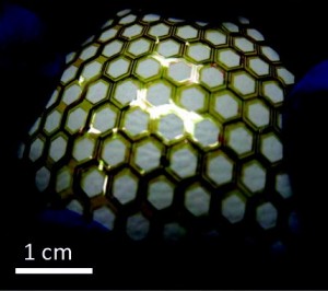 |
| Optical image of flexible and stretchable thin film transistor array covering a baseball shows the mechanical robustness of this backplane material for future plastic electronic devices. |
Abstract:
Imprinting electronic circuitry on backplanes that are both flexible and stretchable promises to revolutionize a number of industries and make "smart devices" nearly ubiquitous. Among the applications that have been envisioned are electronic pads that could be folded away like paper, coatings that could monitor surfaces for cracks and other structural failures, medical bandages that could treat infections and food packaging that could detect spoilage. From solar cells to pacemakers to clothing, the list of smart applications for so-called "plastic electronics" is both flexible and stretchable. First, however, suitable backplanes must be mass-produced in a cost-effective way.
New Path to Flex and Stretch Electronics: Berkeley Lab Researchers Develop Solution-based Fabrication Technique
Berkeley, CA | Posted on December 13th, 2011Researchers with the U.S. Department of Energy (DOE)'s Lawrence Berkeley National Laboratory (Berkeley Lab) have developed a promising new inexpensive technique for fabricating large-scale flexible and stretchable backplanes using semiconductor-enriched carbon nanotube solutions that yield networks of thin film transistors with superb electrical properties, including a charge carrier mobility that is dramatically higher than that of organic counterparts. To demonstrate the utility of their carbon nanotube backplanes, the researchers constructed an artificial electronic skin (e-skin) capable of detecting and responding to touch.
"With our solution-based processing technology, we have produced mechanically flexible and stretchable active-matrix backplanes, based on fully passivated and highly uniform arrays of thin film transistors made from single walled carbon nanotubes that evenly cover areas of approximately 56 square centimeters," says Ali Javey, a faculty scientist in Berkeley Lab's Materials Sciences Division and a professor of electrical engineering and computer science at the University of California (UC) Berkeley. "This technology, in combination with inkjet printing of metal contacts, should provide lithography-free fabrication of low-cost flexible and stretchable electronics in the future."
Javey is the corresponding author of a paper in the journal NanoLetters that describes this work titled "Carbon Nanotube Active-Matrix Backplanes for Conformal Electronics and Sensors." Co-authoring this paper were Toshitake Takahashi, Kuniharu Takei, Andrew Gillies and Ronald Fearing.
With the demand for plastic electronics so high, research and development in this area has been intense over the past decade. Single walled carbon nanotubes (SWNTs) have emerged as one of the top contending semiconductor materials for plastic electronics, primarily because they feature high mobility for electrons - a measure of how fast a semiconductor conducts electricity. However, SWNTs can take the form of either a semiconductor or a metal and a typical SWNT solution consists of two-thirds semiconducting and one-third metallic tubes. This mix yields nanotube networks that exhibit low on/off current ratios, which poses a major problem for electronic applications as lead author of the NanoLetters paper Takahashi explains.
"An on/off current ratio as high as possible is essential for reducing the interruption from pixels in an off-state," he says. "For example, with our e-skin device, when we are pressure mapping, we want to get the signal only from the on-state pixel on which pressure is applied. In other words, we want to minimize the current as small as possible from the other pixels which are supposed to be turned off. For this we need a high on/off current ratio."
To make their backplanes, Javey, Takahashi and their co-authors used a SWNT solution enriched to be 99-percent semiconductor tubes. This highly purified solution provided the researchers with a high on/off ratio (approximately 100) for their backplanes. Working with a thin substrate of polymide, a high-strength polymer with superior flexibility, they laser-cut a honeycomb pattern of hexagonal holes that made the substrate stretchable as well. The holes were cut with a fixed pitch of 3.3 millimeters and a varied hole-side length that ranged from 1.0 to 1.85 millimeters.
"The degree to which the substrate could be stretched increased from 0 to 60-percent as the side length of the hexagonal holes increased to 1.85 mm," Takahashi says. "In the future, the degrees of stretchability and directionality should be tunable by either changing the hole size or optimizing the mesh design."
Backplanes were completed with the deposition on the substrates of layers of silicon and aluminum oxides followed by the semiconductor-enriched SWNTs. The resulting SWNT thin film transistor backplanes were used to create e-skin for spatial pressure mapping. The e-skin consisted of an array of 96 sensor pixels, measuring 24 square centimeters in area, with each pixel being actively controlled by a single thin film transistor. To demonstrate pressure mapping, an L-shaped weight was placed on top of the e-skin sensor array with the normal pressure of approximately 15 kilo Pascals (313 pounds per square foot).
"In the linear operation regime, the measured sensor sensitivity reflected a threefold improvement compared with previous nanowire-based e-skin sensors reported last year by our group," Takahashi says. "This improved sensitivity was a result of the improved device performance of the SWNT backplanes. In the future we should be able to expand our backplane technology by adding various sensor and/or other active device components to enable multifunctional artificial skins. In addition, the SWNT backplane could be used for flexible displays."
This research was supported in part by the DOE Office of Science and in part by the National Science Foundation.
####
About Berkeley Lab
Lawrence Berkeley National Laboratory addresses the world�s most urgent scientific challenges by advancing sustainable energy, protecting human health, creating new materials, and revealing the origin and fate of the universe. Founded in 1931, Berkeley Lab�s scientific expertise has been recognized with 12 Nobel prizes. The University of California manages Berkeley Lab for the U.S. Department of Energy�s Office of Science. For more, visit www.lbl.gov.
For more information, please click here
Contacts:
Lynn Yarris
(510) 486-5375
Copyright © Berkeley Lab
If you have a comment, please Contact us.Issuers of news releases, not 7th Wave, Inc. or Nanotechnology Now, are solely responsible for the accuracy of the content.
Bookmark:


| Related Links |
![]() For more information about the research of Ali Javey, visit the Website at:
For more information about the research of Ali Javey, visit the Website at:
| Related News Press |
News and information
![]() Quantum computer improves AI predictions April 17th, 2026
Quantum computer improves AI predictions April 17th, 2026
![]() Flexible sensor gains sensitivity under pressure April 17th, 2026
Flexible sensor gains sensitivity under pressure April 17th, 2026
![]() A reusable chip for particulate matter sensing April 17th, 2026
A reusable chip for particulate matter sensing April 17th, 2026
![]() Detecting vibrational quantum beating in the predissociation dynamics of SF6 using time-resolved photoelectron spectroscopy April 17th, 2026
Detecting vibrational quantum beating in the predissociation dynamics of SF6 using time-resolved photoelectron spectroscopy April 17th, 2026
Flexible Electronics
![]() Flexible sensor gains sensitivity under pressure April 17th, 2026
Flexible sensor gains sensitivity under pressure April 17th, 2026
![]() MXene nanomaterials enter a new dimension Multilayer nanomaterial: MXene flakes created at Drexel University show new promise as 1D scrolls January 30th, 2026
MXene nanomaterials enter a new dimension Multilayer nanomaterial: MXene flakes created at Drexel University show new promise as 1D scrolls January 30th, 2026
![]() Flexible electronics integrated with paper-thin structure for use in space January 17th, 2025
Flexible electronics integrated with paper-thin structure for use in space January 17th, 2025
![]() Beyond wires: Bubble technology powers next-generation electronics:New laser-based bubble printing technique creates ultra-flexible liquid metal circuits November 8th, 2024
Beyond wires: Bubble technology powers next-generation electronics:New laser-based bubble printing technique creates ultra-flexible liquid metal circuits November 8th, 2024
Thin films
![]() Tiny nanosheets, big leap: A new sensor detects ethanol at ultra-low levels January 30th, 2026
Tiny nanosheets, big leap: A new sensor detects ethanol at ultra-low levels January 30th, 2026
Laboratories
![]() Researchers develop molecular qubits that communicate at telecom frequencies October 3rd, 2025
Researchers develop molecular qubits that communicate at telecom frequencies October 3rd, 2025
Govt.-Legislation/Regulation/Funding/Policy
![]() Quantum computer improves AI predictions April 17th, 2026
Quantum computer improves AI predictions April 17th, 2026
![]() Metasurfaces smooth light to boost magnetic sensing precision January 30th, 2026
Metasurfaces smooth light to boost magnetic sensing precision January 30th, 2026
![]() New imaging approach transforms study of bacterial biofilms August 8th, 2025
New imaging approach transforms study of bacterial biofilms August 8th, 2025
Chip Technology
![]() A reusable chip for particulate matter sensing April 17th, 2026
A reusable chip for particulate matter sensing April 17th, 2026
![]() Metasurfaces smooth light to boost magnetic sensing precision January 30th, 2026
Metasurfaces smooth light to boost magnetic sensing precision January 30th, 2026
Nanotubes/Buckyballs/Fullerenes/Nanorods/Nanostrings/Nanosheets
![]() Tiny nanosheets, big leap: A new sensor detects ethanol at ultra-low levels January 30th, 2026
Tiny nanosheets, big leap: A new sensor detects ethanol at ultra-low levels January 30th, 2026
![]() Enhancing power factor of p- and n-type single-walled carbon nanotubes April 25th, 2025
Enhancing power factor of p- and n-type single-walled carbon nanotubes April 25th, 2025
![]() Chainmail-like material could be the future of armor: First 2D mechanically interlocked polymer exhibits exceptional flexibility and strength January 17th, 2025
Chainmail-like material could be the future of armor: First 2D mechanically interlocked polymer exhibits exceptional flexibility and strength January 17th, 2025
![]() Innovative biomimetic superhydrophobic coating combines repair and buffering properties for superior anti-erosion December 13th, 2024
Innovative biomimetic superhydrophobic coating combines repair and buffering properties for superior anti-erosion December 13th, 2024
Nanomedicine
![]() A fundamentally new therapeutic approach to cystic fibrosis: Nanobody repairs cellular defect April 17th, 2026
A fundamentally new therapeutic approach to cystic fibrosis: Nanobody repairs cellular defect April 17th, 2026
![]() New molecular technology targets tumors and simultaneously silences two �undruggable� cancer genes August 8th, 2025
New molecular technology targets tumors and simultaneously silences two �undruggable� cancer genes August 8th, 2025
![]() New imaging approach transforms study of bacterial biofilms August 8th, 2025
New imaging approach transforms study of bacterial biofilms August 8th, 2025
![]() Electrifying results shed light on graphene foam as a potential material for lab grown cartilage June 6th, 2025
Electrifying results shed light on graphene foam as a potential material for lab grown cartilage June 6th, 2025
Discoveries
![]() Quantum computer improves AI predictions April 17th, 2026
Quantum computer improves AI predictions April 17th, 2026
![]() Flexible sensor gains sensitivity under pressure April 17th, 2026
Flexible sensor gains sensitivity under pressure April 17th, 2026
![]() A reusable chip for particulate matter sensing April 17th, 2026
A reusable chip for particulate matter sensing April 17th, 2026
![]() Detecting vibrational quantum beating in the predissociation dynamics of SF6 using time-resolved photoelectron spectroscopy April 17th, 2026
Detecting vibrational quantum beating in the predissociation dynamics of SF6 using time-resolved photoelectron spectroscopy April 17th, 2026
Announcements
![]() A fundamentally new therapeutic approach to cystic fibrosis: Nanobody repairs cellular defect April 17th, 2026
A fundamentally new therapeutic approach to cystic fibrosis: Nanobody repairs cellular defect April 17th, 2026
![]() UC Irvine physicists discover method to reverse �quantum scrambling� : The work addresses the problem of information loss in quantum computing system April 17th, 2026
UC Irvine physicists discover method to reverse �quantum scrambling� : The work addresses the problem of information loss in quantum computing system April 17th, 2026
Food/Agriculture/Supplements
![]() New imaging approach transforms study of bacterial biofilms August 8th, 2025
New imaging approach transforms study of bacterial biofilms August 8th, 2025
![]() SMART researchers pioneer first-of-its-kind nanosensor for real-time iron detection in plants February 28th, 2025
SMART researchers pioneer first-of-its-kind nanosensor for real-time iron detection in plants February 28th, 2025
Energy
![]() Sensors innovations for smart lithium-based batteries: advancements, opportunities, and potential challenges August 8th, 2025
Sensors innovations for smart lithium-based batteries: advancements, opportunities, and potential challenges August 8th, 2025
![]() Simple algorithm paired with standard imaging tool could predict failure in lithium metal batteries August 8th, 2025
Simple algorithm paired with standard imaging tool could predict failure in lithium metal batteries August 8th, 2025
Textiles/Clothing
![]() Protective equipment with graphene nanotubes meets the strictest ESD safety standards March 25th, 2022
Protective equipment with graphene nanotubes meets the strictest ESD safety standards March 25th, 2022
![]() Polymer fibers with graphene nanotubes make it possible to heat hard-to-reach, complex-shaped items February 11th, 2022
Polymer fibers with graphene nanotubes make it possible to heat hard-to-reach, complex-shaped items February 11th, 2022
![]() Flexible material shows potential for use in fabrics to heat, cool July 3rd, 2020
Flexible material shows potential for use in fabrics to heat, cool July 3rd, 2020
Solar/Photovoltaic
![]() Spinel-type sulfide semiconductors to operate the next-generation LEDs and solar cells For solar-cell absorbers and green-LED source October 3rd, 2025
Spinel-type sulfide semiconductors to operate the next-generation LEDs and solar cells For solar-cell absorbers and green-LED source October 3rd, 2025
![]() KAIST researchers introduce new and improved, next-generation perovskite solar cell November 8th, 2024
KAIST researchers introduce new and improved, next-generation perovskite solar cell November 8th, 2024
![]() Groundbreaking precision in single-molecule optoelectronics August 16th, 2024
Groundbreaking precision in single-molecule optoelectronics August 16th, 2024
![]() Development of zinc oxide nanopagoda array photoelectrode: photoelectrochemical water-splitting hydrogen production January 12th, 2024
Development of zinc oxide nanopagoda array photoelectrode: photoelectrochemical water-splitting hydrogen production January 12th, 2024
|
|
||
|
|
||
| The latest news from around the world, FREE | ||
|
|
||
|
|
||
| Premium Products | ||
|
|
||
|
Only the news you want to read!
Learn More |
||
|
|
||
|
Full-service, expert consulting
Learn More |
||
|
|
||