|
Interview with Mike Thompson, Business Development Manager, Nanotechnology at FEI Company
Thompson has been actively engaged throughout his career in creating tools that enable Nanotechnology. Following university, he joined the Electron Optics division of Philips. After running the Philips Electron Optics Global sales operations, he transferred to the United States and served as vice president at Philips Electron Optics North American within the sales and service divisions. Following the FEI / Philips merger in 1997 he moved to the west coast and served as vice president of Marketing, Sales and Service operations - helping lay the foundation of the business processes that have contributed to the company's success.
In his current function he is engaged in promoting and supporting FEI's ventures and strategies to better serve the new opportunities and challenges that the Nanotechnology era presents.
Thompson has a B.Sc. (Hons) in Materials Science from the University of Surrey, and a Ph.D. from Cambridge University, England.
FEI Company is a leading, global supplier of tools that can image, characterize and micro machine materials at the nanoscale.
|
NN: "Nanotechnology" is an oft-abused term; what definition do you use?
Your oft-abused comment is justified as the term "Nanotechnology" has a chameleon quality and shifts according to the environment in which it is placed; now as our awareness of Nanotech becomes mature we need to be more specific.
The "Nano" prefix is not the problem, being universally understood as the factor 10 to the power -9. The unit is the meter, in [English metre], and the symbol for nanometer is "nm."
The interest and considerable investment associated with the nanotechnology rests in the fact that there is a transitions zone in the properties of matter as one shifts from atoms to bulk materials. The zone in which properties change rapidly is in the linear dimensional range of approximately 1nm to 100nm, this range is often quoted in definitions. As range is an approximation we can capture its meaning by using the term "nanoscale". The objective of nanotechnology is new, and is to functionalize this size/shape property dependence of nanoscale matter. This approach differs from past, current and future engineering which has the objective of functionalizing the "invariant properties" of bulk matter.
Many definitions of "Nanotechnology" are misleading as they can include "science" as a component of the definition. This is at best a convenience as much of what we read about today relates to science at the nanoscale. Here we should emphasize that nanoscale research is essential work as we cannot efficiently functionalize events at the nanoscale until we can understand, and characterize, their properties. The amount of research and engineering which is required to commercialize Nanotechnology is a huge undertaking and has probably been underestimated. While science is a precursor to the creation of a potential product, the contribution is one of the enablement and as should not be incorporated in the definition of "Nanotechnology."
This preamble leads to the definition:
"Nanotechnology incorporates all tools and techniques which lead to the industrial or commercial application of the properties of matter at the nanoscale."
This definition accentuates the true meaning of "technology" - namely the need to apply the knowledge gained by science and engineering in a practical way. It is pragmatic in that it implies the size dependant properties of materials at the nanoscale but does not make it a necessary condition.
A shift in the precision of the definition is needed as the current and sustained high level of government investment in Nanotechnology in countries outside of the USA is focused, involves industry, and is directed towards product creation. In general the purpose of technology is to create new products, and products drive economies. The role of science in the new developing economies is coupled to serve the purpose of economic growth. Any definition of "Nanotechnology" we use in the USA should not attempt to confuse or obscure this reality.
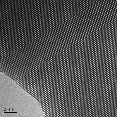
An aberration-free image of atoms of gold produced by the FEI Titan 300 kV transmission electron microscope. The gold atoms are spaced ~ 0.2nm apart (2 Ångströms). Copyright © FEI
Click on image for larger version.
|
NN: What is the key to success in the "tools of the trade" industry?
Success as a tool maker has the same requirements as in all commercial endeavors in that we need to create opportunities for our customers to be successful. Our core technologies of electron and ion optics enables use to build microscopes that can continuously image material from that perceived by the eye to the atomic level. Our challenge is to take this core technology and identify economically significant arenas for our tools. To be commercially viable, the tools need to provide solutions to current unresolved problems, or anticipate and remove obstacles in the path of the knowledge. Some products evolve and are driven by a customer-driven technology push. The most successful products involve deep applications knowledge of a problem to be solved, and a strong technology-pull process. This is the combination that creates new tools and new markets. The approach carries high risk and requires a high level of confidence at all levels in the organization to be successful. The latter process represents the most exiting times for a tool maker as one is trying to introduce solutions to customers just as a problem is beginning to emerge. This is a fine-tuned process - if one is too early one burns time and R&D funds, and if one is too late one loses market share. FEI Company has been successful in introducing new product platforms.
The introduction of the DualBeam tools, which combine imaging and micro-fabrication, has moved microscopy from era's of passive data recording to active manipulation of matter at the nanoscale. This tool is used in scientific, institutional and industrial R&D and has made a profound contribution to our ability to advance nanoscience and nanotechnology.
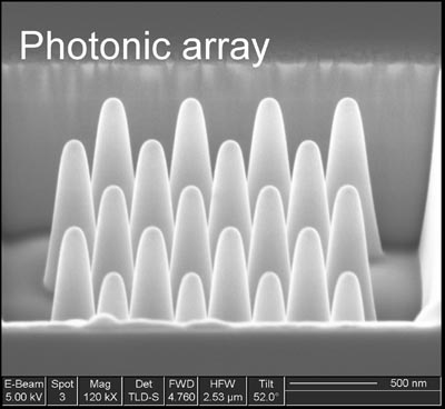
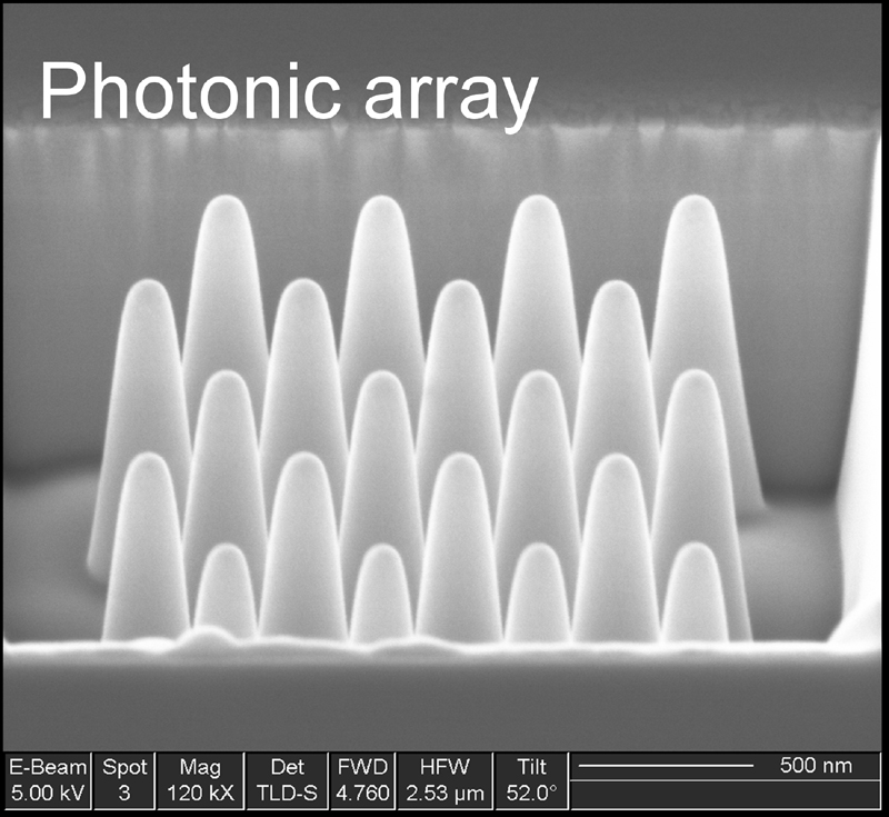
FEI DualBeam Micromachined prototype photonic array. The radii of the cones are ~ 100nm. Copyright © FEI
Click on image for larger version.
|
NN: High resolution imaging is one of the keys to success in nanoelectronics and materials science; what are some of the tools that FEI has developed / is developing in these areas, and what advantages do they bring to research labs?
The study, development and commercial application of materials science has been hindered in the past by a number of major bottlenecks associated with high resolution electron microscopy. These bottlenecks have included the difficulty in being site-selective in the cross-section of a material, and the problem of preparing materials without introducing artifact.
In addition, obstacles have included the support and transfer of a minute sample into the microscope, the inability to conduct volume studies of bulk materials in a Scanning Electron Microscope [SEM] and for the Transmission Electron Microscope [TEM] the inability of to quickly and consistently prepare a sample thin enough to be electron transparent. The problems increase for brittle materials [ceramics, semiconductors and minerals], porous materials or composites with soft and hard phases. The old solution for the Semiconductor industry was to cleave a wafer in order to check the wafer cross-section for production control. This process was haphazard and expensive as wafers were destroyed.
The second factor was the need to transfer the sample into SEM to examine the cross-section. The DualBeam tool, which FEI created, solved all of the prior problems as it allows direct SEM imaging of a site-specific, cross-sectioning without the need to destroy the wafer. The most recent advancement of this technology is to remove and prepare a TEM sample from a minute volume of material. This new technology extends the resolution down to the atomic level which is necessary to for the production control of IC device interfaces. The DualBeam tool has and will continue to enable the Semiconductor & Data Storage industries to improve and then sustain higher yield levels in production. The DualBeam tool is in fact a versatile micro-fabrication device in which the ion beam and gas chemistry provide the fabrication capability and the electron beam the capability for imaging and analysis to the nanoscale. The DualBeam tool originated as a solution for industry. FEI has since created a range of models where design and specifications are adapted to multiple-user, multiple-application requirements of research, prototyping and development and the budgets of university, institutional and industrial laboratories. The market for the DualBeam products is buoyant and continues to grow rapidly.
The most recent product technology that FEI introduced is a Transmission Electron Microscope, which has an image resolution of less than 0.1nm [>1 Ångstrom]. This technology advance includes two new correctors - one of which is a monochromator which removes fluctuations in the electron beam wavelength, and the other which corrects for spherical aberration of the magnetic lenses. These technologies, when used in combination, take the resolution of the microscope to its theoretical limit. The benefits are improvements in the image resolution, easy interpretation as the images of atomic structures need no software correction, and an increased spatial resolution or sensitivity of chemical analysis.
This new platform is called the Titan and it's the highest resolution microscope in the world. This platform will be developed further by FEI, who is a major contractor in the "TEAM" project funded by the US Department of Energy. The "TEAM" project is directed by a consortium of US-based scientists and has the objective of creating a unique transmission electron microscope that will target a resolution of 0.05nm and be installed in 2008.
The need for higher resolution is driven by Nanoscience and Nanotechnology. Both science and engineering need investigative and metrology tools to characterize materials that contain dimensions already at the atomic level. As atoms and atomic spacings have dimensions in the range of 0.1 to 0.5nm we need tools with an even higher resolution to study them; the Titan platform is designed to fulfill this new requirement.
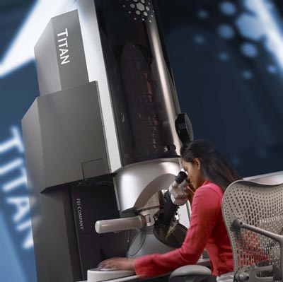
FEIs Titan scanning/transmission electron microscope (S/TEM) is the worlds most advanced, commercially-available microscope, yielding atomic-scale imaging. The Titan is dedicated to corrector and monochromator technologies and was designed for optimum stability, which enables sub-Ångström imaging of nanostructures in both TEM and STEM modes. Copyright © FEI
Click on image for larger version.
|
NN: How do you interact with clients (existing and potential) to develop new tools?
Today the ability to advance in many technical fields relies on better and/or faster tools to get the job done. This makes the communication between the tool maker and the researcher or the production engineer essential. This need requires in turn that FEI employ persons who know and understand the language, the challenges and the constraints of professionals in all fields in which we do business. As microscopy is a mainstream technique in all the life and material sciences and an essential technique for R&D and production, we employ a large number of graduate and Ph.D. specialists trained in each of these fields. These applications specialists serve as an "internal" customer. By "internal" customer we mean someone who knows and understands a specific part of our client base and can, as a result, communicate appropriate new developments and application solutions. This specialist-to-specialist dialogue also aids FEI in identifying trends and issues in that field that we, as tool makers, need to address. Once we have identified a new development, we continue to work with the top people in the field to specify and build new tools. An interesting aspect of the specification is the design of the human interface. As using a microscope relies on the vision and decision making of the operator over long periods of time, a great deal of effort is directed to the ergonomics and the software programming of the control panels.

FEIs Nova NanoLab is a versatile, high-performance DualBeam (FIB / SEM) designed to support the diverse imaging, analytical and sample preparation/modification demands of the high-end lab market. Its precision stage, versatile specimen chamber and DualBeam and gas chemistry technologies allow researchers to analyze, characterize, machine and prototype a wide range of samples on the nanoscale. The easy-to-use DualBeam software enables researchers to conceive and implement complex tasks quickly. Copyright © FEI
Click on image for larger version.
|
NN: What benefits come from being located in Oregon?
Oregon is an attractive balance of business, academic and living environment. Our industrial neighbors include the Intel Rondler Acres site and HP in Corvallis - both of which operate world class nanoscale development and production centers. Genetech has just announced that it plans to build a facility nearby. We benefit from our good relation with ONAMI which is a consortia of Oregon-based universities and institutes that have worked to create a new model for the way in which universities and institutes can share their activities and resources and connect with the industry.
Here in the Pacific Northwest, our proximity to California, as the #1 Nanotech State, and our proximity to the Asia-Pacific economies are considered a benefit. Oregon offers an attractive and compact scenic combination of high desert, mountains, the Columbian gorge and its accessible coastal range. A national magazine recently voted Portland as the best place to live, and Hood River in the gorge as the most active town in the U.S. The state is without doubt a great place to both work and play.
NN: How and why is FEI involved with the 2006 Safer Nano Conference?
FEI was a sponsor of the meeting, has members in the organizing committee and employees who are making presentations. Our desire for involvement in this new forum is at a number of different levels. First and foremost we are directly involved as a manufacturer of tools for Nanotech in the safety and monitoring issues associated with this terrain. We need to educate ourselves and be informed on emergent issues that affect us as an employer and as a distributor of tools whose customers are at work in this new field.
On another level we are in a unique position to contribute and educate others as to the nature of particulates and methods by which they can be individually characterized. The question is "What is the best practice to allow a characterization process to be both statistically significant and economically viable?" We are also aware of the potential for political debate that "Nanotechnology" needs to be regulated. A shared concern is that any legislation would be premature, and could impact the competitiveness of U.S. industry in creating new nanotech-based economies. Today both industry and society are acutely aware of the need to work in harmony. For a corporation, this means proactively identifying issues and contributing to the process of self-regulation. Precedent already exists. The semiconductor industry, for instance, has created both a model and an example of how an advanced technology can regulate its affairs in a socially responsible manner.
NN: By your estimation, how large (in terms of $US) is the nanotech tools market today? How does that compare to 10 years ago, and how will it compare to 10 years from now?
In 1995, the "nanotools" market was under $US 300 Million US. The total Nanotech tools served available market in 2005 was close to $US 1 Billion. Market growth is expected to be roughly 14% per year through 2008. Predictions beyond this point are speculative and will depend upon the rate of adoption rate of tools by industry as nanoscience-based products move from prototyping through to production.
Company Profile 
Headquarters Location: Hillsboro, Oregon
Manufacturing Facility Locations:
Hillsboro, Oregon, US
Eindhoven, The Netherlands
Brno, Czech Republic
Subsidiaries:
Knights Technology
Ticker Symbol (if applicable): Nasdaq: FEIC
Year Incorporated: 1973
Brief History
1949 Philips Electron Optics introduces it 's first commercial transmission electron microscope (TEM).
1971 FEI is founded to provide high-purity, oriented single crystal materials for field emission research.
1982 FEI ships first LMI focusing column.
1983 FEI ships first electrostatically focused electron column. Micrion is founded to develop ion beam systems for mask repair.
1989 FEI ships the first complete ion beam (FIB) workstation.
1990 Philips Electron Optics introduces SEM for 6-inch semiconductor wafers.
1993 The first DualBeam (FIB/SEM) workstation is produced by FEI and Philips Electron Optics.
1996 Philips Electron Optics acquires ElectroScan and its ESEM technology.
1997 FEI and Philips Electron Optics merge. First in-line DualBeam for wafer fab shipped.
1999 FEI acquires Micrion Corporation and integrates product lines and operations.
2000 First small-stage DualBeam launched.
2001 First monochromator TEM.
2004 FEI breaks the 1 Ångström Barrier with a 200kV Tecnai with monochromator and cs correction.
2005 FEI Introduces Titan S/TEM, the world's most powerful commercial microscope with sub-Angstrom resolution
Industry Segment: Nanotechnology Tools for NanoResearch & Industry, NanoElectronics and NanoBiology
Products: FIB, SEM, TEM, S/TEM systems and software. FEI's Tools for Nanotech, featuring focused ion- and electron-beam technologies, deliver 3D characterization, analysis and modification capabilities with resolution down to the sub-Ångstrom level and provide innovative solutions for customers working in NanoBiology, NanoResearch and NanoElectronics. Users of FEI products benefit from faster time to data and discovery, shortened development cycles and faster production ramps, enabling them to get their innovations to market in less time and with less cost With R&D centers in North America and Europe, and sales and service operations in more than 50 countries around the world, FEI is bringing the nanoscale within the grasp of leading researchers and manufacturers and helping to turn some of the biggest ideas of this century into reality.
Vahé A. Sarkissian
President and CEO
Vahé was appointed President and CEO of FEI Company in May 1998 and Chairman of the Board in 2002.
Previously, Vahé was President and CEO of Metrologix Inc., an electron beam metrology company that was acquired by KLA. Prior to Metrologix, Mr. Sarkissian was President and COO of Silicon Valley Group, and was President and CEO of SVG Lithography Systems, a subsidiary of SVG, where he led the Micrascan Step and Scan Deep UV lithography business. Prior to SVG he was Vice President of Data General Corporation and was responsible for the Semiconductor and telecommunication products Divisions where he led a major telecommunications venture with Nippon Telephone and Telegraph. Mr. Sarkissian was also instrumental in the incubation of Actel and Power Integration at Data General. He has held several technical and management positions with semiconductor companies, including AMD where he was a key founding member of the memory and microprocessor products businesses. He has also served on the boards of several high tech start up companies. Mr. Sarkissian holds a B.S.E.E. from Northrup University and an M.S.E.E. From the University of Santa Clara.
Peter Frasso
Executive Vice President and Chief Operating Officer
Peter joined FEI as Executive Vice President and Chief Operating Officer in May, 2005.
Mr. Frasso most recently was Senior VP of Global Operations for Brooks Automation. Prior to Brooks, Peter was the interim CEO of LightPointe Communications, Inc., and also served as the LightPointe Europe executive, responsible for the company's worldwide manufacturing operations. Before that, he held a variety of management positions for 17 years at Varian Associates, where the business he was responsible for was a finalist for the Malcolm Baldridge Award and was twice named Industry Week's Best Plant in America. He has a degree in Mechanical Engineering from Northeastern University.
Raymond A. Link
Executive Vice President & Chief Financial Officer
Ray joined FEI in his current role in July 2005.
Prior to joining FEI, Ray had been the chief financial officer of TriQuint Semiconductor since 2001, having come to TriQuint with the merger of Sawtek Inc. He was the CFO of Sawtek for six years, and was also the CFO of Hubbard Construction for eight years. He holds an MBA from the Wharton School, is a graduate if the State University of New York at Buffalo and is a CPA.
Robert S. Gregg
Executive Vice President of Worldwide Sales and Service
Bob was named to his current position at FEI in May 2005. Prior to that, he was Executive Vice President and Chief Financial Officer of FEI beginning in January 2004.
For two years prior to joining FEI, Bob was a founding executive at SiPrian, Inc., a Portland-based semiconductor start-up. From 1999 through 2002, he was with Unicru, Inc., a leading provider of hiring management software systems, where he was originally a board member and subsequently became President and CEO. From 1983 to 1999, he was with Sequent Computer Systems while the company grew from start-up to over $800 million in revenue, and where he was Senior Vice President and Chief Financial Officer. Before Sequent, he was with Price Waterhouse.
Bob is a graduate of The University of Oregon, with a B.S. in Finance and Accounting.
# of Employees: 1,600
# of Patents: 318
Revenue in previous years:
2005 $ 427 Million
2004 $ 466 Million
2003 $ 361 Million
Contact Information
FEI Company
Global Headquarters
5350 NE Dawson Creek Drive
Hillsboro, Oregon 97124
USA Tel: 503-726-7500
Fax: 503-726-7509
www.feicompany.com
Recent News
March 8, 2006: FEI and Sidec Tackle Validation of Drug Targets
March 6, 2006: BASF Chooses FEI System for Nanoparticle R&D
March 2, 2006: FEI Sponsors 2006 Safer Nano Conference
January 31, 2006: FEI's Titan(TM) S/TEM Receives Industry Honors
December 13, 2005: FEI Company and PDF Solutions(R) Release Powerful New Semiconductor Defect Analysis Solution
November 30, 2005: FEI Introduces New Cryo Sample Prep Tool for Organic Samples
November 10, 2005: FEI Installs World's Most Powerful Commercial Microscope at Ohio State University
|

|
Building The Winning Start-Up Team: Part 3 of 6
By Bo Varga
|
Introduction: Bo Varga has recruited senior technical and executive talent for high technology companies since 1979. Bo is looking for other senior technical and executive recruiting assignments and currently searching for a Director of Multi-Scale Computation Modeling.
Article 1 Covered: Why Hire an External Recruiter? (Click here for a quote, and to buy.)
Article 2: Building The Winning Start-Up Team: Performance Requirements
Entrepreneurs, start-up teams, investors, and recruiters often intersect to match a startup with the experienced business management required for success. Different perspectives & needs & communication styles as well as individuals egos can lead to power struggles that can make or break a company. Many startups usually have a standard set of weak spots in their initial management team - a lack of customer focus, entrepreneurs with little to no background in launching or heading a corporation, or technologists that cannot drive a business as well as develop a technology and get a product to market. Even companies with the strongest potential and IP can become an unattractive investment decision if the right management team isn't in place and if a cooperative team environment is not established & maintained.
Click here to read (for free) the rest of last month's report in full.
Article 3: The Recruiting Process
Article: This article addresses the actual recruiting process an entrepreneur or team can use and the knowledge, background and reference checking to establish baseline trust in a new team member.
Objectives: Upon completion of this article you will understand how to develop a recruiting process and build an overall understanding of a candidate's ability to meet performance requirements as well as the importance of reference checking using a protocol.
Whether building a small team or a large team, one way to work efficiently and to avoid hiring mistakes - especially costly for a start-up - is to develop and use a formal recruiting protocol. While multi-talented individuals with a wealth of experience are not rare, the focus should be on the relevant needs of the company.
A common mistake is to rely on external recruiters to submit candidates and let each hiring manager or the entrepreneur handle hiring. This process often results in uneven hiring, with very strong people in one area, say engineering, and weak people in another, say marketing.
A formal recruiting protocol can avoid much wasted time and energy and money as well as many hiring mistakes. A template that can be adapted to your needs follows:
1: RECRUITING PROTOCOL
- Establish position requirements & job description based on performance goals / desired outcomes, business experience, knowledge base, education, company business model & company culture - include all relevant people in this task, however the hiring manager should drive the process. And the perfect should not be the enemy of the good. I have seen 10 page documents - the goal should be a 1-page document, possible 2 pages.
- Review requirements, revise as needed, agree on compensation package - base salary, bonus, equity, relocation and other special benefits - and take a second look, ideally let a weekend pass before completing this task. And for senior positions review with Board of Directors, Board of Advisors, Investors, Corporate Lawyers, or other outside parties with an interest in the company but not involved in day-to-day operations.
- Get company agreement on recruiting process including who schedules the candidate, greets the candidate, "sells" the candidate on company history and goals and achievements, and who manages the candidate through the recruitment process, including candidate debrief and follow up post interview. This is often an external recruiter, whether working in house or only present to shepherd the candidate. If an external recruiter is not used the responsible person may be the hiring manager - but once a core team is in place a HR manager or specialist is best for this role. In the situation where an external recruiter is not used, a specific person needs to be designated to shepherd each candidate interview.
- Signoff on position requirement & recruiting process - each position needs signoff by the hiring manager and the recruiting team needs to signoff on the process
- Review & sign off on contract for services if external recruiter is used, otherwise designated team member can be substituted when a recruiter is mentioned for the balance of this article
- Recruiter generates a pool of candidates and identifies top candidates - while this can be done by use of personal networks, advertising on the internet on sites such as tinytechjobs.com, etc. we recommend team recruiting only where it is financially impossible to hire a recruiter. The recruiting task takes bandwidth that most nano start-ups can better devote to the product development, release, sales, and support.
- In depth interview of top candidates by recruiter - these are screening interview PRIOR to an in-house interview and can be done by phone and preferably is done via face meetings off site. This way obviously unsuitable candidates, but who have good paper, are screened out prior to burning team bandwidth.
- Recruiter presents candidate profiles - how they track position requirement - CVs - and notes from outside interviews.
- Recruiter sets up interviews and prepares candidates for process and confirms sequence and timing to meet with all team members who will interview the candidate.
- Recruiter present in person during initial interview of candidates
- Recruiter debriefs team and candidate and communicate feedback to both
- Recruiter works with hiring manager and team to select target candidate(s) with company
- Second set of interviews with candidate(s) is optional but often necessary
- Recruiter debrief both parties and communicates feedback
- Company identifies target candidates and appropriate compensation package envelope - least and most to offer for base, bonus, stock, non-standard benefits such as relocation, education allowance, etc.
- Recruiter or hiring manager conducts depth reference checking for target candidate(s), based on reference protocol - as adapted to company needs
- Relevant team reviews references and revisit references as needed
- Recruiter participate in negotiations / communications as required to close
In Article 2: Building the Start-Up Team: The Importance of Performance Requirements I noted that: "Past performance measured by relevant metrics is the single best indicator of ability to meet performance goals." The obvious question is how to determine past performance and create trust within the team about the skills, knowledge, experience, and character of the candidate and the candidate's fit with the corporate culture?
One important method is reference checking. Ideally candidates for senior positions will submit six (6) references, that is two direct reports, two peers, and two hiring managers or project manager or people to whom they reported or who managed the candidate at past engagements.
Educational degrees, publications, patents, and past positions should be checked as a matter of course - while many companies will not give out details of past employment, the fact that a candidate was employed can always be verified and the tile or position can also be verified. The candidate should have references from recent positions - the prior five years - if he or she does not, this is a red flag.
Internet searches on the candidate should always be done, in particular by linking the candidate's name with the educational institution, publication, patent, and past employers.
Red flags that I have found during internet searches include both criminal and civil legal actions that are normally a red flag - as well as "resume escalation", claiming positions, responsibility, and authority that was "deflated" during an internet search.
Even for candidates that come from the team's personal network, references should be checked. Following is a protocol I have successfully used on many executive and senior technical recruiting assignments. When talking with references it is important to evaluate the reference, their tone of voice, how quickly or how slowly they answer questions, questions they choose not to answer, and whether questions are answered shortly or in some detail.
2: Reference Checking Protocol (adapt questions to company needs)
Reference Check for: Candidate Name
Submitted to: Hiring Manager & Company
Reference Name (all reference information comes from candidate)
Reference Contact Information:
Current Title/Position:
Reference Title/Position:
Current Company:
Reference Company:
Introduction: Hello, my name is Bo Varga & CANDIDATE NAME gave me your name as a Professional Reference. I'd appreciate about 30 - 45 minutes of your time for a confidential reference. Is this a good time to call you? If not, is there a better time to call you, when you can talk? Please note that your reference will be confidential.
I work with Silicon Valley Nano Ventures in CA, recruiting for a client in Silicon Valley. Our client is an early stage nanotechnology company, focused on bringing TYPE OF products to market, focused on APPLICATIONS in MARKET OR INDUSTRY. Our client is looking for a CEO to grow the company from early revenue to $25+ million sales within 5 years. As part of that process, CANDIDATE NAME will be required to raise equity in the $10 - $30 million range & to assemble a management team to complement the founders. What I'd like to do is to get your observations & opinions regarding Candidate's management skills, the scope of his past assignments, his team building skills, his funds raising ability, and his customer facing skills. Please feel free to comment at any length. Also, our client may want to call on you for some additional information. And I may need to call again as a follow up. Is this all right with you?
Naturally the introduction will need to be written to reflect the position to be filled and the company that wants to hire.
- How long did Candidate work with you and at which company?
- Was this a contract or permanent position and what was Candidate's title(s) or role(s)?
- What was your working relationship with Candidate? (hiring manager, direct supervisor, co-worker/lateral, direct report, company director, if other, please define)
- Were you familiar with Candidate's assignments - his performance goals?
- What was the primary mission of his team, what outcomes were they to achieve?
- What was the secondary mission?
- What was the technical environment?
- What functional areas was Candidate responsible for?
- What were the major projects or tasks that he worked on?
- In your opinion, what are his greatest strengths as a manager or executive?
- In your opinion, were there any areas where he could improve his skills?
- Can you give me your observations on Candidate's client interface skills, that is his customer facing skills?
- Can you give me your observations regarding Candidate's success at closing major contracts, strategic alliances, or other important revenue generating relationships?
- Do you have direct knowledge regarding Candidates ability to acquire funding or financing required to grow a business, from corporate, VC, investment banking, or other sources?
- Can you give me your opinion regarding Candidate's effectiveness in raising money from venture capitalists or other sources to grow a business.
- Do you have any knowledge regarding Candidate's effectiveness in working with a Board of Directors, either as a member or as a senior corporate officer reporting to the Board?
- From the first month you worked together or became familiar with Candidates work, what first impressions still remain?
- Why did he leave the assignment or the company for which you are giving a reference?
- Did you learn anything from him during the time you worked together?
- What was his most significant accomplishment while you worked together or for the period for which you are giving a reference?
- What budgets were Candidate's responsibility on the reference assignment?
- Do you know approximately the dollar levels of those budgets?
- How many direct and indirect reports was he responsible for?
- How many of these reports were senior level, VP or Director or the similar?
- Can you tell me how intense or stressful the work environment was on a scale of 1 to 10, with 10 the most intense & stressful, such as 24x7 mission critical service with an unstable IS/IT platform & unhappy customers?
- To your knowledge did Candidate meet or exceed project goals?
- Were deadlines met and tasks completed on time?
- On budget?
- Do you know how Candidate expanded/kept current his skill set?
- Do you know how Candidate expanded/kept current his team's skill sets?
Now please give your ratings for Candidate as Superior, Very Good, Good, or Average for Industry in the following areas. I appreciate any comments you have. Please feel free to speak at length.
After each question I ask Superior, Very Good, Good, or Average for Industry - and when I get the response I ask if the reference has any additional comments.
- In your opinion, how effective was Candidate in meeting his hiring plan?
- How effective was he in attracting senior management & executive talent?
- How would you rate his interaction with technical founders?
- How do you rate his track record of delivering against his promises?
- How do you rate his Leadership Skills
- How do you rate his Customer Facing Skills?
- How do you rate his ability to raise equity or funding for projects?
- How do you rate his Technical Ability?
- How do you rate his Commitment to Work?
- How do you rate his Dependability?
- How do you rate his Integrity?
- How do you rate his team recruiting, building, motivating skills?
- How do you rate his effectiveness in handling conflict among team members?
- How do you rate his effectiveness in handling conflict between functional departments?
- How do you rate his communication skills with non-technical upper management?
- How do you rate his working relationship with his bosses and/or the BOD?
- How do you rate his communication skills with professional audiences?
- How do you rate his communication skills with the financial community, that is VCs, investment bankers, CFOs, corporate directors, research analysts, & others involved in funding or valuing companies?
- Would you work with him again or rehire?
- Is there anything else about Candidate that you could tell me to help me understand his strong points & possible areas for improvement both as an employee & an executive?
- Finally, would you rate your overall reference for Candidate as Very Positive, Positive, Slightly Positive, Neutral, or Negative?
Thank you for your time. I appreciate your help & professional courtesy. If you need to reach me again my phone number is 650-747-9238 and I can be reached 7AM to 10PM, 7 days per week, PST.
Next month I will revisit the recruiting process and focus primarily on building trust - a key ingredient in building the winning nano team.
© Copyright 2006 Bo Varga
|
Bo Varga is the Managing Director of Silicon Valley Nano Ventures.
Bo has 30 years business development and team building experience. His primary focus is to bring money to companies via angel, corporate, or VC investment, strategic alliances, development partnerships, or OEM sales. Bo has operations, sales, & marketing management experience in computer software & peripherals and in leading edge reconfigurable computing systems. He has worked with wireless, nanotechnology, reconfigurable computing, information technology, & ecommerce companies in team-building or business development roles.
He has helped executives, investors, and Boards of Directors for software, hardware, IS/IT, molecular engineering, & wireless companies by finding key team members and consultants for both technical & business positions.
His experience includes working as a strategic consultant to develop & implement marketing plans & presentations, with a specific focus on affiliate & event marketing to close business transactions. His focus since 2000 is on building global nanotechnology business networks via the nanoSIG & various nanotechnology conferences, forums, and symposiums. He is Chair of the NanoMaterials & Manufacturing Forum. Since 2001 he has organized over 60 nanotechnology events. His education includes a BA & MA from the University of Chicago and the MBA program in Accounting at UC Berkeley.
For more information on his work, see www.nanoSIG.org, www.USnano.biz.
He can be reached at bvarga@USnano.biz, or 650-747-9238 for more information.
|
Quotes
"One of the exciting yet challenging aspects of nanotechnology investing is the rich variety of opportunities -- from new tools that are essential to some aspect of getting a nanotechnology to market in the near term; to materials that disrupt the economics of a market that is large today; to the really cool science that may have a commercial application some day." —David Aslin, a West Coast partner at 3i link
"Nanotechnology is nothing less than a revolution, and today Oregon is leading the nation in tools for nanotechnology," said Kohrt. "Today, nanotechnology accounts for less that one-tenth of 1 percent of the gross national product [under $12 billion], whereas by 2014, it will be 15 percent, or $2.6 trillion. And 50 percent of the microelectronics market will involve nanotechnology." As many as 10 million people will work in nanotech by then, he said. —Carl Kohrt, chief executive at Battelle link
"Tools are the most important part of this business at this stage," Lagally says. "Tools enabled the nanotech revolution. Being able now to see and manipulate the things at that scale allows us to do something. The first stage is always some discovery, and then some tool to make it happen for everybody. Once the tools are in place, then the research can progress into fabricating materials and devices, and products that use them." —Max Lagally, a materials science professor, UW-Madison
Aggregate survey responses indicated that the U.S. Pacific region leads the nation in development of diverse nanotechnology products and application markets that are being pursued for potentially disruptive economic, social, environmental and military advantage. The U.S. leads the world in the generation and commercialization of nanoscale materials, manipulation tools and measurement innovations being applied to initially benefit the consumer products, digital storage, photovoltaic and semiconductor manufacturing industries. Myriad new applications of advanced nanocoatings, nanofilms and nanoparticles are being developed for introduction in the near-term (3-5 years) on a broader range of durable goods, consumer electronics and medical products. Nanoproduct applications are also being developed for the next generation semiconductor, energy, chemical catalysis and pharmaceutical/biomedical products. 2005 NCMS Survey of Nanotechnology in theU.S. Manufacturing Industry
"Advancements in enabling tools are supporting the drive into nanoscale research and development reaching down into the atomic scale," said Matt Harris, vice president of worldwide marketing for FEI Company. "Scientists have never before had the ability to understand and control nanomaterials as they can today. This ability, coupled with shared industry focus on safety and management of these materials will encourage the pursuit of nanotechnology to proceed safely and with rational discussion."
Molecular nanotechnology promises to usher in the next Industrial Revolution and replace our entire manufacturing base with a new, radically precise, less expensive, and more flexible way of making products. These pervasive changes in manufacturing will leave virtually no product, process, or industry untouched. To be sure, nanotechnology has the potential to disrupt entire industries while leading to the creative destruction of current business models. It has already dramatically changed the competitive landscape of many industries worldwide including advanced materials/composites, aerospace/defense, automotive, energy, life sciences, medicine, electronics and semiconductors. Yet the future potential of nanotechnology depends on creating the tools that will enable us to effectively position molecules and build complex structures with atomically precise control. Every aspect of basic nanoscale science and the commercial production of nanotechnology will rely---first and foremost---on the capacity of these tools, instruments, metrology devices, and modeling/simulation applications to measure, sense, fabricate, and manipulate matter at the atomic level. Nanomanufacturing Conference & Exhibits
The markets for nano materials, tools and equipment for nanoelectronics totaled US$1,827 million in 2005 and are forecasted to reach $4,219 million by the year 2010, according to Global Nanoelectronics Markets and Opportunities, a comprehensive new market research report that is now available from SEMI. link
There can be no doubt that a modern and effective research infrastructure is critical to maintaining U.S. leadership in science and engineering. New tools have opened vast research frontiers and fueled technological innovation in fields such as biotechnology, nanotechnology, and communications. The degree to which infrastructure is regarded as central to experimental research is indicated by the number of Nobel Prizes awarded for the development of new instrument technology. During the past twenty years, eight Nobel prizes in physics were awarded for technologies such as the electron and scanning tunneling microscope, laser and neutron spectrography, particle detectors, and the integrated circuit. - National Science Board, December 2002
link
At the very heart of nanotechnology and its future promise are the tools, instruments, metrological devices, and modeling/simulation applications that will enable us to effectively position matter and build intricate structures with atomically-precise control. Many novel instruments have been created and today they are accelerating the pace of developing innovative top-down and bottom-up manufacturing processes. Soon they will enable us to fabricate materials, components, devices, and products on a more cost-effective, highly-repeatable, and replicable basis. Nanomanufacturing Conference & Exhibits
News
"Tools" News: January 01, 2006 - March 31, 2006
Using Probes to Control Chemistry - Molecule by Molecule
Brookhaven National Laboratory March 31, 2006 Using probes originally designed to detect and image topographical features on surfaces, scientists at the U.S. Department of Energys Brookhaven National Laboratory have demonstrated the ability to initiate and spatially localize chemical reactions on the submicron scale. They have been able to reliably manipulate chemistry on a very, very small scale in contrast to normal beaker-type reactions carried out in bulk. Such site-selective chemistry, taken down to the molecule-by-molecule level, could lead to new ways to etch small-scale electronic circuits, the development of extremely sensitive chemical sensors, as well as a better understanding and control of chemical reactions such as those used to convert sunlight into electricity in solar cells.
One important benefit of this technique is that it is environmentally friendly, Wong says, using no electric current or potentially harmful reaction conditions. Furthermore, the technique has such high specificity that it offers the potential for single-molecule detection and analysis a benefit with possible applications in refined chemical sensor technology. Such sensors might be able to detect as little as a single molecule of a potentially hazardous material released, for example, in a terror attack.
IBM develops method to control atom-scale magnetism
EETimes March 31, 2006 IBM scientists have developed a new technique, called spin-excitation spectroscopy, to explore and control magnetism at its fundamental atomic level. The method promises to be important not only in the quest to understand the operation of future computer circuit and data-storage elements as they shrink toward atomic dimensions, but also to lay the foundation for new materials and computing devices that leverage atom-scale magnetic phenomena. "We can now position atoms and then measure and control their magnetic interactions within precisely designed structures."
Nanometrics files suit against Nova
EETimes March 30, 2006 Nanometrics (Milpitas, Calif.) claimed Nova (Rehovoth, Israel) was infringing Nanometrics U.S. Patent Number Re. 34,783.
International NANOSPIN project
NT-MDT March 30, 2006
NRC Neutron Reflectometry Workshop
National Research Council Canada March 30, 2006 NRC Canadian Neutron Beam Centre in Chalk River are running a one-day workshop this Summer on neutron reflectometry: a powerful tool for research in nanostructured materials.
Algorithm works out nanoparticle structure
nanotechweb March 29, 2006 Since nanoparticles don't have long-range crystalline order, it's hard to use conventional crystallographic methods to look at their structure. But now researchers at Michigan State University, US, have come up with an algorithm that enables them to determine the three-dimensional structure of a nanoparticle from one-dimensional X-ray or neutron diffraction data.
Making measurements at one billionth of a metre
Imperial College London March 28, 2006 Developing new techniques for making precise measurements at the scale of one billionth of a metre is the focus of a new £5.6 million award for the London Centre for Nanotechnology (LCN).
BudgetSensors® Launches BS-Tipcheck
openpr.com March 27, 2006 BudgetSensors®, a Bulgarian manufacturer of silicon and silicon nitride probes for Atomic Force Microscopes (AFM) announces the launch of a new calibration standard the BS-Tipcheck.
Veeco Introduces 5th Generation SPM Technology
businesswire March 27, 2006 Veeco Instruments Inc. (Nasdaq: VECO), a leading supplier of instrumentation to the research and nanoscience community, today announced the launch of two new scanning probe microscope (SPM) products, the MultiMode(R) V SPM and the Dimension(R) V SPM for a broad range of research and industrial applications.
Millbrook Scientific up on order wins
sharecast.com March 24, 2006 The latest deals include the group's first sale to Australia where the University of Melbourne has purchased a NanoTest system for conducting advanced experiments at the nanoscale level.
Expansion of electron microscope sales area
laboratorytalk.com March 22, 2006 With the appointment of Paul Allen as electron microscope distributor manager, Greece, Turkey, Israel, United Arab Emirates and South Africa now have local distribution outlets for Hitachi's comprehensive range of scanning and transmission electron microscopes.
FEI Certified Tools Program to be Launched at SEMICON China
news2u.net March 21, 2006 FEI
Company (Nasdaq: FEIC) will launch a Certified Tools program for the Chinese market during SEMICON China in Shanghai this week. The program, which features fully-tested and warranted factory-refurbished FEI systems, will provide China-based customers greater flexibility, capital equipment acquisition leverage and added confidence as research institutions and industrial customers across China continue to invest in nanoscale development and commercialization.
Doctor Russells AFM course participation
NT-MDT March 21, 2006 NT-MDT company to provide equipment for laboratory use
Building a Nano-Friendly Facility
rdmag.com March 21, 2006 With the increasing emphasis on research and development in nano-scale subjectsincluding nanomedicine, nanofabrication, and the imaging of nano-scale structures in bioengineering, proteomics/genomics, and other emerging fieldsfacilities must be planned and designed to meet the complex physical requirements of highly sophisticated imaging and analysis equipment while efficiently meeting the needs of the scientists who use these instruments. In particular, the use of MRI, NMR, and SPECT-CT instrumentation, and the installation of nanofabrication clean suites raise challenging planning and design issues, including space planning, structural capacity, vibration and noise isolation, magnetic and radiofrequency shielding, and instrument quench exhaust. Here is a look at the issues and practical solutions.
Allen expands scope network
electronicstalk.com March 20, 2006 Hitachi High-Technologies has announced a major expansion in sales territories for its electron microscopes. With the appointment of Paul Allen as Electron microscope Distributor Manager, Greece, Turkey, Israel, United Arab Emirates and South Africa now have local distribution outlets for Hitachi's comprehensive range of scanning and transmission electron microscopes.
Science and Innovation Awards
innovations-report.com March 20, 2006 Funding has been awarded to build the UKs research base in the areas of nanometrology, statistics, plasma physics and the Mathematics-Computer Science interface. (Including:)
Imperial College London and University College London - £5.6 million for Professor Tim Jones (Imperial) and Professor Gabriel Aeppli (UCL) to develop new tools for nanoscale characterisation and metrology.
University of Strathclyde and Kings College London - £4.3 million to advance the emerging field of nanometrology, for applications in molecular science, medicine and manufacture.
Aviza Technology Announces Multiple System Order From SMIC
businesswire March 20, 2006 Aviza Technology, Inc. (Nasdaq:AVZA), a supplier of advanced semiconductor equipment and process technologies for the global semiconductor, compound semiconductor, nanotechnology and other related markets, today announced that it has received multiple system orders from Semiconductor Manufacturing International Corporation ("SMIC", NYSE: SMI and HKSE: 0981.HK) for the RVP-300plus(TM) and RVP-550(TM) thermal processing systems.
UD researcher's device monitors airborne nanoparticles
University of Delaware March 20, 2006 With a deep interest in the effects of air pollution on human health and global climate change, a University of Delaware researcher has developed a nanoaerosol mass spectrometer that can characterize microscopic airborne particles.
A primary use of the device, which was developed by Murray V. Johnston III, University of Delaware professor of chemistry and biochemistry, in cooperation with postdoctoral fellow Shenyi Wang and graduate student Christopher A. Zordan, is to characterize human exposure to such nanoparticles.
Science and Innovation Awards
eurekalert.org March 17, 2006 Imperial College London and University College London - £5.6 million for Professor Tim Jones (Imperial) and Professor Gabriel Aeppli (UCL) to develop new tools for nanoscale characterisation and metrology.
University of Strathclyde and King's College London - £4.3 million to advance the emerging field of nanometrology, for applications in molecular science, medicine and manufacture.
Carl Zeiss & Seiko partner on product portfolio
fabtech.org March 16, 2006 Carl Zeiss Nano Technology Systems (NTS), a division of Carl Zeiss SMT, and SII NanoTechnology (SIINT), a subsidiary of Seiko Instruments have made a bold move to become a leading force in the emerging field of nanotechnology instrumentation.
Fisher Scientific Expands Presence in Molecular Diagnostics
businesswire March 16, 2006 Fisher Scientific International Inc. (NYSE: FSH) announced two transactions that will significantly enhance its capabilities in molecular diagnostics. Fisher has entered into a definitive agreement to acquire privately held Athena Diagnostics, Inc., from Behrman Capital for $283 million in cash. Simultaneous with its acquisition of Athena, Fisher has entered into an agreement to purchase 9 percent of Nanogen, Inc. (Nasdaq: NGEN) for $15 million in cash.
MOSFET-Embedded Microcantilevers
sciencemag.org March 16, 2006 A promising approach for detecting biomolecules follows their binding to immobilized probe molecules on microfabricated cantilevers.
NanoHUB: Gateway to Nanoscience
hpcwire.com March 16, 2006 The nanoHUB is a Web-based initiative spearheaded by the NSF's Network for Computational Nanotechnology (NCN). Its purpose is to serve as a resource for research and education in the areas of nanoelectronics, nano-electromechanical systems (NEMS), and their application to nano-biosystems. The NCN has a mission to connect theory, experiment, and computation in a way that makes a difference to the future of nanotechnology. While addressing challenges in nanotechnology NCN researchers produce new algorithms, approaches, and software tools with capabilities not yet available commercially. As part of the NSF's infrastructure for the National Nanotechnology Initiative, the NCN engages the community through workshops and seminars and novel educational resources. The nanoHUB is a source of on-line resources including a unique web-based computational user facility that puts research-grade software in the hands users across the globe.
Non-Contact Atomic Force Microscopy
Institute of Physics March 15, 2006 The 14 April issue of Nanotechnology contains selected papers from the 8th International Conference on Non-Contact Atomic Force Microscopy (NC-AFM) held at Bad Essen, Germany last summer.
$500k to study integrating nano into silicon semiconductors
University of Texas at Austin March 15, 2006 A University of Texas at Austin microelectronics researcher has received $500,000 from the Department of Defense to research ways to use nanotechnology to overcome hurdles that might halt the march of the silicon-based integrated circuit.
Molecular Foundry Dedication at Berkeley Lab
ascribe March 15, 2006 Lawrence Berkeley National Laboratory will signal its most significant entry into the nano-age when it dedicates a six-story, 94,000-square-foot facility known as the "Molecular Foundry" on Friday, March 24, at 10:30 a.m.
Ultratech Receives Multiple Lithography System Orders
prnewswire March 15, 2006 Ultratech, Inc. (Nasdaq: UTEK), a leading supplier of lithography and laser-processing systems
used to manufacture semiconductors and nanotechnology devices, today announced that Siliconware Precision Industries Co. Ltd. (SPIL).
Surface Technology Systems Cluster Tools
prnewswire March 14, 2006 Surface Technology Systems plc (STS) (LSE: SRTS), a leader in plasma process technologies required in the manufacturing and packaging of advanced electronic devices, today announced that, in recent weeks, it has received multiple orders worth over 1 million pounds Sterling for its cluster tools.
FEI's Automated 3D Cyrstallography Featured at PITTCON
prnewswire March 13, 2006 FEI Company (Nasdaq: FEIC) will feature its EBS3 DualBeam(TM) solution for rapid serial sectioning and 3D crystallographic reconstructions of materials at this week's PITTCON conference in Orlando. The fully integrated solution, utilizes an FEI DualBeam (FIB/SEM) system with an EBSD detector and advanced automation software.
Advance Nanotech Researchers Test Novel Optic Device
businesswire March 13, 2006 Advance Nanotech, Inc., (OTCBB:AVNA), the premier provider of financing and support services to expedite the commercialization of nanotechnology discoveries, today announced a breakthrough in its optics and photonics research at the Center for Advanced Photonics and Electronics (CAPE) at the University of Cambridge, UK.
WITec launches new alpha300 microscope generation
WITec March 09, 2006 WITec, a specialist in high-resolution optical and scanning probe microscopy has launched a new modular microscope generation, the alpha300 series. This series includes the Confocal Raman Microscope "alpha300 R", the Scanning Near-field Optical Microscope "alpha300 S" and the Atomic Force Microscope "alpha300 A" all driven by the new fully digital control unit "alphaControl".
UKs Diamond will throw light on key research
ft.com March 09, 2006 Diamond Light Source, as it is known, will produce X-ray, infrared and ultra- violet beams of exceptional brilliance. This highly focused radiation will enable scientists to probe deep into the basic structure of materials, with a vast range of applications from drug design to nanotechnology.
FEI and Sidec Tackle Validation of Drug Targets
prnewswire March 08, 2006 FEI Company (Nasdaq: FEIC) and Sweden-based Sidec Technologies AB today announced that the two companies will collaborate on the commercialization of Protein Tomography solutions and services based on Sidec's proprietary software and intellectual property, and FEI's transmission electron microscopes (TEMs).
Keithley Plays Key Role in Test Standards for Carbon Nanotubes
businesswire March 07, 2006 Keithley Instruments, Inc. (NYSE:KEI), a leader in solutions for emerging measurement needs, announces that its Model 4200 Semiconductor Characterization System conforms to and supports the just-released IEEE standard for electrical testing of carbon nanotubes.
BASF Chooses FEI System for Nanoparticle R&D
prnewswire March 06, 2006 FEI Company (Nasdaq: FEIC) today announced that BASF, the world's leading chemical company, has ordered one of FEI's top-of-the- line DualBeam systems, the Strata(TM) 400. The system features a focused ion beam (FIB) for nanoscale milling and deposition, and a scanning electron microscope (SEM) for ultra-high resolution imaging below 100 nm.
El-Mul gets $1.3 M to develop CNT electron beam sources
El-Mul Technologies March 06, 2006 El-Mul Technologies will participate in a project valued at over $1.3 million to continue development of new electron beam sources based on its proprietary carbon nanotube device. (PDF)
Visual Simulation Solutions for Education
thenanotechnologygroup.org March 06, 2006 Judith Light Feather: Advances in microscopy and optical lenses have opened the window to nature allowing us to see how the world actually works at the atomic level. This scale of science is all-encompassing and demands collaboration between physics, chemistry, biology, engineering and information technology, along with simulation and modeling software technicians.
Company pioneers microscopic technology for commercial testing
gwinnettdailypost.com March 05, 2006 In a laboratory housed at the companys Breckinridge Boulevard headquarters stands the Nano Test, a $225,000 device that enables Vander Wood and others to see clearly at such a small scale.
New power centre for nanotechnology
copcap.com March 05, 2006 ... a joint consortium within nanoscience and nanotechnology between the University of Copenhagen and Technical University of Denmark (DTU).
Bier Receives NSF Funding To Build Mass Spectrometer
Carnegie Mellon University March 04, 2006 Carnegie Mellon University's Mark Bier has received a $546,000 grant from the National Science Foundation's Instrument Development for Biological Research program to build a heavy-ion mass spectrometer. This one-of-a-kind mass spectrometer will characterize with unprecedented sensitivity large biomolecules, such as intact proteins, protein complexes, virus particles and DNA. It may also provide a new tool for analyzing large man-made polymers used in nanotechnology.
Farfield appoints John Parkes as sales manager
laboratorytalk.com March 03, 2006 Farfield Sensors, a specialist in analytical instrumentation for biophysics and nanotechnology, announces the appointment of John Parkes as sales manager.
President's Science Advisor to Visit Keithley Instruments
businesswire March 01, 2006 Keithley Instruments, Inc. (NYSE:KEI), a leader in solutions for emerging measurement needs, announced today it will host a visit on March 2 from Dr. Celia Merzbacher, Executive Director of the President's Council of Advisors on Science and Technology.
Obducat tips nano-imprint for production
EETimes February 27, 2006 The system from Obducat (Malmo, Sweden) is a 200-mm tool said to handle resolutions of 30-nm and below.
Analyzing Air Nanoparticulates
Chemical & Engineering News February 27, 2006 The chemical composition of airborne nanoparticles is largely unknown because of measurement difficulties. Chemists at the University of Delaware, Newark, have now developed a nanoaerosol mass spectrometer that combines an aerodynamic inlet, an ion trap, and a time-of-flight mass analyzer to characterize individual particles smaller than 10 nm.
Ultrafast Imaging
technologyreview February 23, 2006 A novel instrument for scanning and manipulating molecules could open up new possibilities for nanotechnology, promising, among other things, far faster imaging of biomolecules and nanoelectronic materials. The new microscope, invented by researchers at Georgia Tech and Stanford University, could be a dramatic improvement on atomic force microscopy, one of the main tools of nanotechnology.
Zeiss and UCI Develop Research Center
photonics.com February 23, 2006 Carl Zeiss and UCI have established a center for nanotechnology and biotechnology research and advanced materials development.
(Read the full Calit2 release from Nov. '05)
Nanostructures in 3D
Max Planck Institute February 23, 2006 It is the worlds first electron microscope for simultaneously and automatically investigating in three-dimensions the phase content, crystallographic texture, and crystal interfaces of materials - co-designed and put into service at the Department of Microstructure Physics and Metal Forming at the Max Planck Institute for Iron Research in Düsseldorf, Germany. The device contains a high-resolution scanning electron microscope and an -ion-beam microscope. In the past, these two types of microscopes have been used separately; now, they have been integrated into a single instrument together with an arsenal of detectors which can measure electron diffraction patterns and orientations, as well as perform chemical analyses. This allows scientists to see the inner structure of nanomaterials, biological matter, and high-performance steels, in ways that other microscopic procedures cannot - and in full 3D.
Opening bell for JPK School
verivox.de February 21, 2006 February 13 was the opening day of the first JPK Instruments School for atomic force microscopy (AFM). Under the banner AFM user training for biological applications, researchers and scientists from among JPK clients gathered at the companys headquarters in Berlins Bouchéstrasse for the schools first session.
World's Smallest Fiber-Optic Electric Field Probe
japancorp.net February 21, 2006 NEC Corporation today announced the successful development of the world's smallest fiber-optic electric field probe, enabled through the adoption of a nanotechnology process. The newly developed probe consists of an optical fiber and an electro-optical film that is formed at its edge, which acts as a field sensor. As its lateral size of approximately 125 micrometer is equivalent to that of the diameter of an optical fiber, the probe can be inserted into narrow spaces such as the crevice between a ball grid array (BGA) LSI package and a printed circuit board (200 - 300 micrometer), enabling evaluation of the electrical characteristics of high-density packaged electronic circuits on printed circuit boards (PCBs). It can therefore be utilized to create electrical designs for high-density electronic packages toward the realization of low-noise/low-electromagnetic interference (EMI) level circuits.
NanoWorld AG Announces Pyrex-Nitride AFM Probe
prweb February 20, 2006 NanoWorld today officially announced its new Pyrex-Nitride AFM probe. The Pyrex-Nitride probe combines silicon nitride cantilevers and tips with the proven glass chip concept.
Photonic Nanojets Open Door to Visible-Light Ultramicroscopy
newswiretoday.com February 19, 2006 A recent paper by researchers at Northwestern University in Illinois provides a physical explanation for the phenomenon wherein the backscattering of light by dielectric particles of sizes between 100 and 1 nm is enhanced by 711 orders of magnitude.
(Read the details)
Obducat's CEO comments on the annual accounts for 2005
Obducat February 17, 2006 Obducats industrial order for a NIL (nano-imprint lithography) machine after the end of the reporting period shows that a very important milestone has been reached: NIL technology can be used in mass production. The customer manufactures optical components that are part of a consumer electronics product from Samsung which will be launched on the market in May. It is also interesting that the customer who placed the order now for a further NIL machine had originally expected to place a second order first in autumn 2006. This breakthrough is the result of a very hard and committed effort on the part of Obducats personnel over a long period.
Nanofabrication Laboratory at Chalmers now accessible
idw-online.de February 17, 2006 One of the most advanced university cleanrooms in the world, the Nanofabrication Laboratory, at the Department of Microtechnology and Nanoscience, MC2, at Chalmers University of Technology, in Göteborg, Sweden, is now offering European Universities and SME:s access, free of charge, to advanced micro- and nanotechnology fabrication resources.
Spectroscope twist sees single molecules
EETimes February 15, 2006 Putting a new spin on a standard technique, researchers at the University of Illinois at Urbana-Champaign replaced single-molecule fluorescence spectroscopy with an absorption technique that has the same resolution as atomic-force microscopy, today's highest resolution for observing surface features.
Veeco Victorious in 2006?
fool.com February 15, 2006 Dan Bloom: I bought a few shares of Veeco Instruments (Nasdaq: VECO) a while back and just filed them away, expecting that a cyclical wave would eventually take my shares for a ride. But even after Tuesday's 11% shellacking, I only have a small gain so far. After digging through the results that Veeco posted on Monday, it looks like the cyclical uptick I'm hoping for won't occur in 2006. While the company's fourth-quarter and full-year results show improvements, Veeco's weak guidance for the first quarter of this year raises question marks.
Mass production breakthrough for Obducats NIL technology
Obducat February 15, 2006 In view of the need to increase production capacity, one of Obducats US customers has placed an order for an additional industrial NIL machine (Nano Imprint Lithography). Using the NIL technology provided by Obducat, the customer produces optical components forming part of a consumer electronics product supplied by Samsung, which will be introduced on the market in May 2006. This is a breakthrough for Obducats NIL technology at mass production.
Agilent Technologies Parametric Testers Selected
businesswire February 14, 2006 Agilent Technologies Inc. (NYSE:A) today announced that the Crolles2 Alliance (for Nanotechnology Joint Development Program) has purchased three Agilent 93000 Pin Scale testers and four 4073 advanced parametric testers for research, development and industrialization of CMOS process technologies.
MOCVD tool for Reel to Reel Superconducting Films
Structured Materials Industries February 13, 2006
Nanoscience Experts to Highlight ICMI Meeting in Austin
SEMATECH February 13, 2006
New Device Revolutionizes Nano Imaging
Georgia Tech February 09, 2006 Georgia Tech researchers have created a highly sensitive atomic force microscopy (AFM) technology capable of high-speed imaging 100 times faster than current AFM. This technology could prove invaluable for many types of nano-research, in particular for measuring microelectronic devices and observing fast biological interactions on the molecular scale, even translating into movies of molecular interactions in real time. The research, funded by the National Science Foundation and the National Institutes of Health, appears in the February issue of Review of Scientific Instruments.
Tegal Receives Repeat Order
businesswire February 08, 2006 Tegal Corporation (Nasdaq:TGAL) today announced that a leading wireless component supplier has placed a multiple system order for 901ACS diode plasma etch systems featuring the Advanced Control System.
Ambios Technology, Inc. acquires Quesant Instrument Corp.
Ambios Technology February 08, 2006
Lumera Reaches Agreement with the Medical University
businesswire February 06, 2006 Lumera Corporation (Nasdaq:LMRA), an emerging leader in the field of nanotechnology, announced today that it has executed a letter of intent with the Medical University of South Carolina to purchase its newly released ProteomicProcessor(TM) Biosensor instrument. Additionally, MUSC and Lumera announced they will co-develop a new protein chip, based on Lumera's NanoCapture(TM) HPT technology, which will be aimed at the growing drug discovery and toxicology market.
Tiny flag is no small achievement
dallasnews.com February 04, 2006 Two University of Texas at Dallas students believe they have created the world's tiniest flag. Their three-dimensional version of the Texas flag is so small it can only be seen with an electron microscope. About 1,000 of the tiny banners could stand on the head of a pin.
R&D profile: Advanced Technology Institute
electronicsweekly.com February 03, 2006 Research: Nanoelectronics; photonics; ion beam implantation and analysis; and theory and advanced computation
SMI announces additional funding for VLA optical coatings
Structured Materials Industries February 02, 2006
SMI awarded DOE Phase II SBIR to develop p-type ZnO
Structured Materials Industries February 02, 2006
Scientists giddy about comet dust
orovillemr.com February 01, 2006 Armed with state-of-the-art scopes, diamond saws and ion beams, scientists are prying at the invisibly tiny world of primordial space dust to find the original ingredients for everything in our solar system, including us.
Due to billions of dollars invested in nanotechnology and materials science, researchers now have vastly more powerful electron microscopes, ion probes, X-ray machines and other esoteric instruments capable of divining what is inside these leftovers from the formation of our solar system 4.6 billion years ago.
NanoSensors, Inc. Reports Plans
prnewswire February 01, 2006 NanoSensors, Inc. (OTC Bulletin Board: NNSR.OB) reports today on the Company's current course of work and future plans. NanoSensors has recently been in talks with several different companies, universities and patent holders with regard to possible intellectual property acquisition and commercialization transactions.
FEI's Titan(TM) S/TEM Receives Industry Honors
prnewswire January 31, 2006 Within months of its release, FEI's Titan(TM) scanning transmission electron microscope (S/TEM), the world's most powerful, commercially-available microscope, has earned four prestigious awards for its design, performance and innovation. Awards include the coveted iF Design Award bestowed by the International Design Forum (iF) in Hannover, Germany, and the Innovative Product of the Year Award presented by the Oregon Tech Awards in the United States.
Xradia Receives $1.4 Million Grant
businesswire January 31, 2006 Xradia, Inc., a developer and manufacturer of ultra-high-resolution x-ray imaging systems for 3D tomography and nanotechnology applications, today announced receipt of a $1.4 million grant from the National Institutes of Health (NIH) for the development of an ultra-high-resolution x-ray microscope for the three-dimensional imaging of complex biological systems.
Sematech expands presence at UAlbany
ACBJ January 30, 2006 Sematech is opening a $50 million research center at the state University at Albany's College of Nanoscale Science and Engineering. Work at the center, Sematech's second at the UAlbany campus, will focus on extreme-ultraviolet lithography - a radiation process used to produce semiconductors with structures less than 45 nanometers.
Applied Materials hit with $100M lawsuit
ACBJ January 30, 2006 Applied Materials Inc. is facing a $100 million antitrust suit ... alleging Applied Materials froze five microchip equipment refurbishers out of that market.
NANOSENSORS introduces Q30K-Plus Silicon AFM probes
NANOSENSORS January 27, 2006
Osaka University Team Uses Zetasizer Nano
htscreening.net January 27, 2006 A research team in Japan has published work that illustrates the utility of Malvern Instruments Zetasizer Nano particle characterization system in assessing the suitability of a protein sample for crystallization.
Nanometrics buys Accent for $81 million
EETimes January 26, 2006 Metrology-equipment specialist Nanometrics Inc. has signed a definitive agreement to acquire Accent Optical Technologies Inc., a supplier of process control and metrology systems, for $80.9 million in stock.
Innovative 32nm, 22nm Interconnects
businesswire January 24, 2006 Applied Materials, Inc. (Nasdaq:AMAT) and IMEC, Europe's leading independent nanoelectronics and nanotechnology research center, announced today a significant joint effort to develop 32nm and 22nm-node copper/low k interconnect processing technologies using a suite of Applied Materials' most advanced systems.
Picosun's ALD reactor installed at University of Helsinki
Picosun Oy January 24, 2006 University of Helsinki announced that Picosun Oy's SUNALE R-150 ALD reactor has been installed and is performing well at the Laboratory of Inorganic Chemistry
Nanotech research dominates UH contest
University of Houston January 23, 2006 Three Students Take Top Honors in Student Superconductivity Symposium
MU high-tech researchers think small
columbiatribune.com January 22, 2006 Working with powerful particles in tiny packages, an international group of researchers at the University of Missouri-Columbia is hoping to move nanotechnology from the laboratory to the marketplace.
Shubhra Gangopadhyay, the LaPierre Chair professor of electrical and computer engineering, is leading the research on the campus. She is the co-director of the Micro/Nano Systems Technology Center, the first and only research facility of its kind in Missouri.
Antitrust lawsuit targets Applied Materials
EETimes January 20, 2006 Five U.S. companies that refurbish chip-manufacturing equipment have sued industry leader Applied Materials Inc., alleging it engaged in anticompetitive practices by limiting the availability of replacement parts for chip gear.
Møller gives world-class microscope
denmark.dk January 19, 2006 The world's strongest magnifying electron microscope is on its way to the Technical University of Denmark (DTU), promising to make the university a leader in nanotechnology. The microscope will be able to see objects as small as 0.07 nanometers, half the size of a carbon atom.
Purdue engineers solve chaos mystery
Purdue University January 19, 2006 Mechanical engineers at Purdue University have proven that the same sort of "deterministic chaos" behind the baffling uncertainties of the stock market and long-term weather conditions also interferes with measurements taken with a commonly used scientific instrument.
JMAR to Showcase BriteLight(TM) Laser
businesswire January 18, 2006 JMAR Technologies, Inc. (NASDAQ: JMAR) is showcasing its BriteLight(TM) DPSS Laser System at the Photonics West 2006 Conference from January 21 to 26, 2006 at the San Jose Convention Center in San Jose, CA.
Keithley Recognizes 60 Year Milestone of Innovation
businesswire January 17, 2006 Keithley Instruments, Inc. (NYSE:KEI), a leader in solutions for emerging measurement needs, is celebrating this year its 60th year of innovation. Founded in 1946, Keithley today has expanded its measurement portfolio far beyond its patented sensitive DC measurement capabilities to now include additions to its product line with RF (radio frequency) and pulse measurement technologies.
BudgetSensors® Launches New Product Type
BudgetSensors January 17, 2006
New look for nanodetection
physicsweb January 16, 2006 Optical physicists in the US have invented a way of detecting single nanoparticles in real time. Devised by Filipp Ignatovich and Lukas Novotny of the University of Rochester in New York, the new technique involves measuring the amplitude of light scattered from the particles and can detect objects as small as 5 nanometres in diameter. The researchers say the method could be used to detect viruses or to build sensors that provide early warning of biological weapons.
Two international nanotechnology conferences announced
mtbeurope.info January 15, 2006 International Congress on Nanobiotechnology & Nanomedicine (NanoBio 2006), will be held June 19-21, 2006, Hilton Hotel Financial District, San Francisco. www.nanobio2006.com
International Congress of Nanotechnology (ICNT) 2006, October 30-November 2, 2006 in San Francisco. www.nanotechcongress.com
Company seeks out CMUs Biotech lab
cm-life.com January 13, 2006 CMU lab space is now being leased to a growing biotechnology company. Two researchers from the Connecticut based Artificial Cell Technologies, Inc. (ACT) will be stationed in the Dow Science Complex. The biomedical and nanotechnology company develops sophisticated artificial cells through polypeptide engineering.
Smith, Wyden announce federal funds
bend.com January 12, 2006 U.S. Senators Ron Wyden (D-Ore.) and Gordon Smith (R-Ore.) announced that Oregon will soon receive $67.3 million in funding for defense-related projects in Oregon, including significant funding for a number of Oregon nanotechnology projects.
The Oregon Nanoscience and Microtechnologies Institute (ONAMI) would receive $2.5 million for the Nanoelectronics and Nanometrology Initiative, $1.7 million for the safer nanomaterials and nanomanufacturing program, and $1.5 million for the development of miniature tactical energy systems.
Oregon Health and Science University would receive $1.5 million for its Nanotechnology and Health Care center to boost nanotech research efforts across a variety of disciplines.
New look for nanodetection
nanotechweb January 11, 2006 Optical physicists in the US have invented a way of detecting single nanoparticles in real time. Devised by Filipp Ignatovich and Lukas Novotny of the University of Rochester in New York, US, the new technique involves measuring the amplitude of light scattered from the particles and can detect objects as small as 5 nanometres in diameter. The researchers say the method could be used to detect viruses or to build sensors that provide early warning of biological weapons.
Advanced Imaging
advancedimagingpro.com January 11, 2006 The MDA grant, Multispectral Nanoantenna Infrared Sensors, is worth $749,810 and covers the development of nanotechnology operating in infrared bands and ensuing integration with ultrahigh-speed cellular visual microprocessor (CVM), operating at rates beyond 1,000 fps. The ONR grant also involves CVM technology and is worth $299,774. (look under the heading "Add Processing, Storing, Sensing, Then Stir")
Versatile atomic level weight metrology tool from Metryx
fabtech.org January 10, 2006 A new, non-destructive, nanotechnology weight metrology tool has been introduced by Metryx to handle high volume production of 300mm semiconductor wafers.
Carbon Nanoprobes to present at venture series
ACBJ January 05, 2006 Carbon Nanoprobes Inc. of White Plains and EGO7 LLC of New York City will make their pitches on Jan. 25.
Study Moves "Superlens" Closer to Reality
Oregon State University January 05, 2006 Physicists at Oregon State University have made an important advance towards the creation of a functional "superlens" - an extraordinary optical device that would bend light the opposite direction of that done by any natural material. In theory, a superlens might be able to attain visual resolution at the level of the nanometer.
From Our Molecular Future: How Nanotechnology, Robotics, Genetics, and Artificial Intelligence Will Transform Our World, by Douglas Mulhall:
-
What happens to the monetary system when everyone is able to satisfy his own basic material needs at very low cost?
-
How would we use cash when digital manufacturing makes it impossible to differentiate a counterfeit bill or coin from the real thing?
-
What happens to fiscal policy when digital information, moving at light speed, is the major commodity?
-
How fast will monetary cycles move compared to, say, the ten- or twenty-year cycles of the late twentieth century, when products and patents go out of date in a matter of months instead of years?
-
What happens when we don't have to worry about trade or social services for our basic needs, because most of what we need is provided locally with digital manufacturing, and the biggest trade is in information?
-
How do we control the excesses of the ultrarich, the overabundance of the molecular assembler economy, and the challenge to intellectual property laws created by intelligent, inventive machines?
-
What happens if half of all jobs are made redundant every decade?
-
What happens to the War on Drugs when there's no import, export, or transport of contraband because drugs can be manufactured in a desktop machine using pirated software downloaded from the Internet?
-
What happens to democratic controls when individuals can get as rich as small governments in a year or so?
-
What's the relevance of insurance if many things are replaceable at very low capital cost, but liabilities from software are potentially unlimited?
-
How should organized labor react when molecular assemblers and intelligent robots eliminate most manufacturing jobs?
-
What is the nature of work going to be?
-
What happens to land prices when an individual can build a tropical farm under a bubble in North Dakota, and get there from New York in an hour?
-
What happens when everyone can go everywhere, whenever they want, and work from wherever they want?
Return to Top
Useful Links
Our Tool Makers Directory
Return to Top
IN THE NEXT ISSUE
Issue #35 will cover Investing. It will land in your mailbox May 1st, 2006.
Infamous Quotes:
"This 'telephone' has too many shortcomings to be seriously considered as a means of communication. The device is inherently of no value to us." Western Union internal memo, 1876
"Heavier-than-air flying machines are impossible." - Physicist and mathematician Lord Kelvin, President of the British Royal Society, 1895
"Everything that can be invented has been invented." - Charles H. Duell, Director of U.S. Patent Office, 1899
"There is no likelihood man can ever tap the power of the atom." - Robert Milikan, Nobel Laureate in Physics, 1923
"Theoretically, television may be feasible, but I consider it an impossibility-a development which we should waste little time dreaming about." - Lee de Forest, inventor of the cathode ray tube, 1926
"I think there is a world market for maybe five computers." IBM's Thomas Watson, 1943
"Landing and moving around on the moon offer so many serious problems for human beings that it may take science another 200 years to lick them." - Science Digest, August 1948
"Computers in the future may weigh no more than 1.5 tons." Popular Mechanics, 1949
"There is no reason anyone would want a computer in their home." Ken Olsen, Digital Equipment Corp, 1977
And the lesson is? It's a tough game to call.
Need advice? Check out NanoStrategies
© Copyright 1999-2006 7thWave, Inc. All rights reserved. More information on copyright, and disclaimers regarding the content of this newsletter can be found here
|