Home > Press > InnovationLab and Heidelberg collaborate on industrial production of printed and organic sensors: Firms achieve volume and price breakthroughs in manufacture of printed sensors
 |
Abstract:
InnovationLab, an expert in printed and organic electronics, today announced a partnership with Heidelberger Druckmaschinen AG (Heidelberg), world market leader in the manufacturing of printing presses, that will result in the mass production of inexpensive printed and organic sensors, freeing companies to design and produce low-cost customized pressure sensors on an industrial scale for the first time.
InnovationLab and Heidelberg collaborate on industrial production of printed and organic sensors: Firms achieve volume and price breakthroughs in manufacture of printed sensors
Heidelberg, Germany | Posted on August 19th, 2020According to IDTechEx, the market for printed sensors, which includes both organic and flexible sensors, will reach US$4.5B by 2030[i] � opening new use cases in automotive, healthcare, supply chain logistics and other markets. Meeting that level of demand, however, will require a new approach to the design-to-production process of sensors.
�Embarking on the development and industrial production of printed and organic electronics represents a milestone for Heidelberg and for Germany as an industrial player. As we see it, our involvement in this production of high-tech sensors opens up the potential for growth in the two- to three-digit million euro range,� said Rainer Hundsd�rfer, CEO, Heidelberg. �Our partnership with InnovationLab allows us to offer customers quality of design, reliability, a lower bill of materials, and the highest imaginable volumes. In fact, we have the capacity to produce enough sensors to cover a tennis court every hour under a reliable three-shift production system."
�The first step to the widespread adoption of printed and organic sensors is good design, which is one of our historic strengths,� said Luat Nguyen, managing director, InnovationLab. �The second is reliable, high-quality volume production. Our collaboration with Heidelberg fulfills both requirements, enabling us to provide a one-stop shop for printed and organic electronics. Now we can give customers a quick transition from design and feasibility studies through market entry, all the way to mass production. This is our unique Lab2Fab concept.�
Advantages of Printed and Organic Electronics
Until recently, companies have manufactured sensors using conventional semiconductor foundries, which rely on a nine-step process to fabricate each sensor. While well-established, this approach has several downsides: Design-to-production cycles are slow, iteration is costly�as is the per-sensor price�and choice of substrate is limited to rigid materials such as silicon, making such sensors unsuitable for many use cases.
In contrast, printing sensors using roll-to-roll printing methods provides greater choice in functional materials, substrates and deposition methods, offering flexibility of design to accommodate thousands of different applications.
Benefits:
A wide range of materials include organic semiconductors and nanomaterials, (transparent) conductive inks, force- and temperature-sensitive materials allow customers to choose among rigid substrates (e.g., glass, ITO-glass, silicon) and flexible substrates (e.g., PET, PEN, TPU, flexible glass, and others)
Printing sensors only requires a two-step process, saving time and resources�and significantly reducing bill of materials (BOM) costs
Sensors can be printed on flexible, even biodegradable materials, such as textiles�introducing new use cases such as foils of printed sensors that wrap around car batteries to monitor battery health in real-time as well as printed sensors in bandages that monitor the pressure on or moisture of a wound. Printed flexible sensors on food items can both track supply chain conditions like compliance with the cold chain.
####
About InnovationLab
Technical Capabilities
InnovationLab offers an ISO 9001-certified facility that utilizes processes that conform to the IATF 16949 automotive quality standard. Customers have the choice of two production sites, both offering clean rooms, which is important for the quality and reliability of the printing process.
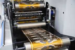
InnovationLab has a highly modified printing press that supports prototyping and pilot production of up to one million (finger-sized) sensors per day. Heidelberg�s production site in Wiesloch, Germany, features a further developed printing press that is solely used for the industrial production of printed sensors, run in a three-shift operation.
For more information, please click here
Contacts:
Readers contact:
Copyright © InnovationLab
If you have a comment, please Contact us.Issuers of news releases, not 7th Wave, Inc. or Nanotechnology Now, are solely responsible for the accuracy of the content.
Bookmark:


| Related News Press |
News and information
![]() Quantum computer improves AI predictions April 17th, 2026
Quantum computer improves AI predictions April 17th, 2026
![]() Flexible sensor gains sensitivity under pressure April 17th, 2026
Flexible sensor gains sensitivity under pressure April 17th, 2026
![]() A reusable chip for particulate matter sensing April 17th, 2026
A reusable chip for particulate matter sensing April 17th, 2026
![]() Detecting vibrational quantum beating in the predissociation dynamics of SF6 using time-resolved photoelectron spectroscopy April 17th, 2026
Detecting vibrational quantum beating in the predissociation dynamics of SF6 using time-resolved photoelectron spectroscopy April 17th, 2026
Organic Electronics
![]() Unveiling the power of hot carriers in plasmonic nanostructures August 16th, 2024
Unveiling the power of hot carriers in plasmonic nanostructures August 16th, 2024
![]() Efficient and stable hybrid perovskite-organic light-emitting diodes with external quantum efficiency exceeding 40 per cent July 5th, 2024
Efficient and stable hybrid perovskite-organic light-emitting diodes with external quantum efficiency exceeding 40 per cent July 5th, 2024
Possible Futures
![]() A fundamentally new therapeutic approach to cystic fibrosis: Nanobody repairs cellular defect April 17th, 2026
A fundamentally new therapeutic approach to cystic fibrosis: Nanobody repairs cellular defect April 17th, 2026
![]() UC Irvine physicists discover method to reverse �quantum scrambling� : The work addresses the problem of information loss in quantum computing system April 17th, 2026
UC Irvine physicists discover method to reverse �quantum scrambling� : The work addresses the problem of information loss in quantum computing system April 17th, 2026
Sensors
![]() Flexible sensor gains sensitivity under pressure April 17th, 2026
Flexible sensor gains sensitivity under pressure April 17th, 2026
![]() Tiny nanosheets, big leap: A new sensor detects ethanol at ultra-low levels January 30th, 2026
Tiny nanosheets, big leap: A new sensor detects ethanol at ultra-low levels January 30th, 2026
![]() From sensors to smart systems: the rise of AI-driven photonic noses January 30th, 2026
From sensors to smart systems: the rise of AI-driven photonic noses January 30th, 2026
![]() Sensors innovations for smart lithium-based batteries: advancements, opportunities, and potential challenges August 8th, 2025
Sensors innovations for smart lithium-based batteries: advancements, opportunities, and potential challenges August 8th, 2025
Announcements
![]() A fundamentally new therapeutic approach to cystic fibrosis: Nanobody repairs cellular defect April 17th, 2026
A fundamentally new therapeutic approach to cystic fibrosis: Nanobody repairs cellular defect April 17th, 2026
![]() UC Irvine physicists discover method to reverse �quantum scrambling� : The work addresses the problem of information loss in quantum computing system April 17th, 2026
UC Irvine physicists discover method to reverse �quantum scrambling� : The work addresses the problem of information loss in quantum computing system April 17th, 2026
Alliances/Trade associations/Partnerships/Distributorships
![]() Chicago Quantum Exchange welcomes six new partners highlighting quantum technology solutions, from Chicago and beyond September 23rd, 2022
Chicago Quantum Exchange welcomes six new partners highlighting quantum technology solutions, from Chicago and beyond September 23rd, 2022
![]() University of Illinois Chicago joins Brookhaven Lab's Quantum Center June 10th, 2022
University of Illinois Chicago joins Brookhaven Lab's Quantum Center June 10th, 2022
Printing/Lithography/Inkjet/Inks/Bio-printing/Dyes
![]() Presenting: Ultrasound-based printing of 3D materials�potentially inside the body December 8th, 2023
Presenting: Ultrasound-based printing of 3D materials�potentially inside the body December 8th, 2023
![]() Simple ballpoint pen can write custom LEDs August 11th, 2023
Simple ballpoint pen can write custom LEDs August 11th, 2023
![]() Disposable electronics on a simple sheet of paper October 7th, 2022
Disposable electronics on a simple sheet of paper October 7th, 2022
|
|
||
|
|
||
| The latest news from around the world, FREE | ||
|
|
||
|
|
||
| Premium Products | ||
|
|
||
|
Only the news you want to read!
Learn More |
||
|
|
||
|
Full-service, expert consulting
Learn More |
||
|
|
||