Home > Press > Spot-welding graphene nanoribbons atom by atom
 |
Abstract:
Scientists at Aalto University and Utrecht University have created single atom contacts between gold and graphene nanoribbons.
Spot-welding graphene nanoribbons atom by atom
Aalto, Finland | Posted on June 13th, 2013In their article published in Nature Communications, the research team demonstrates how to make electrical contacts with single chemical bonds to graphene nanoribbons. Graphene is a single layer of carbon atoms arranged in a honeycomb lattice. It is anticipated to be a revolutionising material for future electronics.
Graphene transistors functioning at room temperature require working at the size scale of less than 10 nanometres. This means that the graphene nanostructures have to be only a few tens of atoms in width. These transistors will need atomically precise electrical contacts. A team of researchers have now demonstrated experimentally how this can be done.
In their article the scientists address the problem by demonstrating how a single chemical bond can be used to make an electrical contact to a graphene nanoribbon.
- We cannot use alligator clips on the atomic scale. Using well-defined chemical bonds is the way forward for graphene nanostructures to realise their potential in future electronics, says Professor Peter Liljeroth who heads the Atomic Scale Physics group at Aalto University.
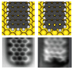
The team used atomic force microscopy (AFM) and scanning tunnelling microscopy (STM) to map the structure of the graphene nanoribbons with atomic resolution. The researchers used voltage pulses from the tip of the scanning tunnelling microscope to form single bonds to the graphene nanoribbons - precisely at a specific atomic location. The pulse removes a single hydrogen atom from the end of a graphene nanoribbon and this initiates the bond formation.
- Combined AFM and STM allows us to characterise the graphene nanostructures atom-by-atom, which is critical in understanding how the structure, the bonds with the contacts and their electrical properties are related, explains Dr Ingmar Swart who leads the team concentrating on STM and AFM measurements at Utrecht University
Combining the microscopy experiments with theoretical modelling, the team developed a detailed picture of the contacted nanoribbon properties. The most significant discovery is that a single chemical bond forms an electronically transparent contact with the graphene nanoribbon - without affecting its overall electronic structure. This may be the key to using graphene nanostructures in future electronic devices, as the contact does not change the intrinsic ribbon properties.
- These experiments on atomically well-defined structures allow us to quantitatively compare theory and experiment. This is a great opportunity to test novel theoretical ideas, concludes Dr Ari Harju, leader of the theoretical team in the project at Aalto University.
The study was performed at Aalto University Department of Applied Physics and at the Debye Institute in Utrecht University. The groups at Aalto are part of the Academy of Finland's Centres of Excellence in "Low Temperature Quantum Phenomena and Devices" and "Computational Nanosciences". Academy of Finland and the European Research Council ERC funded the research.
####
For more information, please click here
Contacts:
Peter Liljeroth
358-503-636-115
Copyright © Aalto University
If you have a comment, please Contact us.Issuers of news releases, not 7th Wave, Inc. or Nanotechnology Now, are solely responsible for the accuracy of the content.
Bookmark:


| Related Links |
| Related News Press |
News and information
![]() Researchers develop molecular qubits that communicate at telecom frequencies October 3rd, 2025
Researchers develop molecular qubits that communicate at telecom frequencies October 3rd, 2025
![]() Next-generation quantum communication October 3rd, 2025
Next-generation quantum communication October 3rd, 2025
![]() "Nanoreactor" cage uses visible light for catalytic and ultra-selective cross-cycloadditions October 3rd, 2025
"Nanoreactor" cage uses visible light for catalytic and ultra-selective cross-cycloadditions October 3rd, 2025
Graphene/ Graphite
![]() Electrifying results shed light on graphene foam as a potential material for lab grown cartilage June 6th, 2025
Electrifying results shed light on graphene foam as a potential material for lab grown cartilage June 6th, 2025
![]() Breakthrough in proton barrier films using pore-free graphene oxide: Kumamoto University researchers achieve new milestone in advanced coating technologies September 13th, 2024
Breakthrough in proton barrier films using pore-free graphene oxide: Kumamoto University researchers achieve new milestone in advanced coating technologies September 13th, 2024
Chip Technology
![]() Lab to industry: InSe wafer-scale breakthrough for future electronics August 8th, 2025
Lab to industry: InSe wafer-scale breakthrough for future electronics August 8th, 2025
![]() A 1960s idea inspires NBI researchers to study hitherto inaccessible quantum states June 6th, 2025
A 1960s idea inspires NBI researchers to study hitherto inaccessible quantum states June 6th, 2025
![]() Programmable electron-induced color router array May 14th, 2025
Programmable electron-induced color router array May 14th, 2025
Nanoelectronics
![]() Lab to industry: InSe wafer-scale breakthrough for future electronics August 8th, 2025
Lab to industry: InSe wafer-scale breakthrough for future electronics August 8th, 2025
![]() Interdisciplinary: Rice team tackles the future of semiconductors Multiferroics could be the key to ultralow-energy computing October 6th, 2023
Interdisciplinary: Rice team tackles the future of semiconductors Multiferroics could be the key to ultralow-energy computing October 6th, 2023
![]() Key element for a scalable quantum computer: Physicists from Forschungszentrum J�lich and RWTH Aachen University demonstrate electron transport on a quantum chip September 23rd, 2022
Key element for a scalable quantum computer: Physicists from Forschungszentrum J�lich and RWTH Aachen University demonstrate electron transport on a quantum chip September 23rd, 2022
![]() Reduced power consumption in semiconductor devices September 23rd, 2022
Reduced power consumption in semiconductor devices September 23rd, 2022
Discoveries
![]() Researchers develop molecular qubits that communicate at telecom frequencies October 3rd, 2025
Researchers develop molecular qubits that communicate at telecom frequencies October 3rd, 2025
![]() Next-generation quantum communication October 3rd, 2025
Next-generation quantum communication October 3rd, 2025
![]() "Nanoreactor" cage uses visible light for catalytic and ultra-selective cross-cycloadditions October 3rd, 2025
"Nanoreactor" cage uses visible light for catalytic and ultra-selective cross-cycloadditions October 3rd, 2025
Announcements
![]() Rice membrane extracts lithium from brines with greater speed, less waste October 3rd, 2025
Rice membrane extracts lithium from brines with greater speed, less waste October 3rd, 2025
![]() Researchers develop molecular qubits that communicate at telecom frequencies October 3rd, 2025
Researchers develop molecular qubits that communicate at telecom frequencies October 3rd, 2025
![]() Next-generation quantum communication October 3rd, 2025
Next-generation quantum communication October 3rd, 2025
![]() "Nanoreactor" cage uses visible light for catalytic and ultra-selective cross-cycloadditions October 3rd, 2025
"Nanoreactor" cage uses visible light for catalytic and ultra-selective cross-cycloadditions October 3rd, 2025
Interviews/Book Reviews/Essays/Reports/Podcasts/Journals/White papers/Posters
![]() Spinel-type sulfide semiconductors to operate the next-generation LEDs and solar cells For solar-cell absorbers and green-LED source October 3rd, 2025
Spinel-type sulfide semiconductors to operate the next-generation LEDs and solar cells For solar-cell absorbers and green-LED source October 3rd, 2025
![]() Rice membrane extracts lithium from brines with greater speed, less waste October 3rd, 2025
Rice membrane extracts lithium from brines with greater speed, less waste October 3rd, 2025
|
|
||
|
|
||
| The latest news from around the world, FREE | ||
|
|
||
|
|
||
| Premium Products | ||
|
|
||
|
Only the news you want to read!
Learn More |
||
|
|
||
|
Full-service, expert consulting
Learn More |
||
|
|
||