Home > Press > Field-Effect Transistors: Self-Assembled Monolayers Create P-N Junctions in Graphene Films
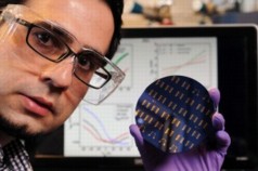 |
| Georgia Tech postdoctoral fellow Hossein Sojoudi holds a wafer containing graphene p-n junctions, while the screen display in the background shows electrical data measured in the devices. (Credit: Gary Meek) |
Abstract:
The electronic properties of graphene films are directly affected by the characteristics of the substrates on which they are grown or to which they are transferred. Researchers are taking advantage of this to create graphene p-n junctions by transferring films of the promising electronic material to substrates that have been patterned by compounds that are either strong electron donors or electron acceptors.
Field-Effect Transistors: Self-Assembled Monolayers Create P-N Junctions in Graphene Films
Atlanta, GA | Posted on December 10th, 2012A low temperature, controllable and stable method has been developed to dope graphene films using self-assembled monolayers (SAM) that modify the interface of graphene and its support substrate. Using this concept, a team of researchers at the Georgia Institute of Technology has created graphene p-n junctions - which are essential to fabricating devices - without damaging the material's lattice structure or significantly reducing electron/hole mobility.
The graphene was grown on a copper film using chemical vapor deposition (CVD), a process that allows synthesis of large-scale films and their transfer to desired substrates for device applications. The graphene films were transferred to silicon dioxide substrates that were functionalized with the self-assembled monolayers.
Information about creating graphene p-n junctions using self-assembled monolayers was presented on November 28, 2012 at the Fall Meeting of the Materials Research Society. Papers describing aspects of the work were also published in September 2012 in the journals ACS Applied Materials & Interfaces and the Journal of Physical Chemistry C. Funding for the research came from the National Science Foundation, through the Georgia Tech Materials Research Science and Engineering Center (MRSEC) and through separate research grants.
"We have been successful at showing that you can make fairly well doped p-type and n-type graphene controllably by patterning the underlying monolayer instead of modifying the graphene directly," said Clifford Henderson, a professor in the Georgia Tech School of Chemical & Biomolecular Engineering. "Putting graphene on top of self-assembled monolayers uses the effect of electron donation or electron withdrawal from underneath the graphene to modify the material's electronic properties."
The Georgia Tech research team working on the project includes faculty members, postdoctoral fellows and graduate students from three different schools. In addition to Henderson, professors who are part of the team include Laren Tolbert from the School of Chemistry and Biochemistry and Samuel Graham from the Woodruff School of Mechanical Engineering. The project team also includes Hossein Sojoudi, a postdoctoral fellow, and Jose Baltazar, a graduate research assistant.
Creating n-type and p-type doping in graphene - which has no natural bandgap - has led to development of several approaches. Scientists have substituted nitrogen atoms for some of the carbon atoms in the graphene lattice, compounds have been applied to the surface of the graphene, and the edges of graphene nanoribbons have been modified. However, most of these techniques have disadvantages, including disruption of the lattice - which reduces electron mobility - and long-term stability issues.
"Any time you put graphene into contact with a substrate of any kind, the material has an inherent tendency to change its electrical properties," Henderson said. "We wondered if we could do that in a controlled way and use it to our advantage to make the material predominately n-type or p-type. This could create a doping effect without introducing defects that would disrupt the material's attractive electron mobility."
Using conventional lithography techniques, the researchers created patterns from different silane materials on a dielectric substrate, usually silicon oxide. The materials were chosen because they are either strong electron donors or electron acceptors. When a thin film of graphene is placed over the patterns, the underlying materials create charged sections in the graphene that correspond to the patterning.
"We were able to dope the graphene into both n-type and p-type materials through an electron donation or withdrawal effect from the monolayer," Henderson explained. "That doesn't lead to the substitutional defects that are seen with many of the other doping processes. The graphene structure itself is still pristine as it comes to us in the transfer process."
The monolayers are bonded to the dielectric substrate and are thermally stable up to 200 degrees Celsius with the graphene film over them, Sojoudi noted. The Georgia Tech team has used 3-Aminopropyltriethoxysilane (APTES) and perfluorooctyltriethoxysilane (PFES) for patterning. In principle, however, there are many other commercially-available materials that could also create the patterns.
"You can build as many n-type and p-type regions as you want," Sojoudi said. "You can even step the doping controllably up and down. This technique gives you control over the doping level and what the dominant carrier is in each region."
The researchers used their technique to fabricate graphene p-n junctions, which was verified by the creation of field-effect transistors (FET). Characteristic I-V curves indicated the presence of two separate Dirac points, which indicated an energy separation of neutrality points between the p and n regions in the graphene, Sojoudi said.
The group uses chemical vapor deposition to create thin films of graphene on copper foil. A thick film of PMMA was spin-coated atop the graphene, and the underlying copper was then removed. The polymer serves as a carrier for the graphene until it can be placed onto the monolayer-coated substrate, after which it is removed.
Beyond developing the doping techniques, the team is also exploring new precursor materials that could allow CVD production of graphene at temperatures low enough to permit fabrication directly on other devices. That could eliminate the need for transferring the graphene from one substrate to another.
A low-cost, low-temperature means of producing graphene could also allow the films to find broader applications in displays, solar cells and organic light-emitting diodes, where large sheets of graphene would be needed.
"The real goal is to find ways to make graphene at lower temperatures and in ways that allow us to integrate it with other devices, either silicon CMOS or other materials that couldn't tolerate the high temperatures required for the initial growth," Henderson said. "We are looking at ways to make graphene into a useful electronic or opto-electronic material at low temperatures and in patterned forms."
This material is based on work supported by the National Science Foundation (NSF) under Grants CHE-0822697, CHE-0848833 and CMMI-0927736 and the Georgia Tech Materials Research Science and Engineering Center (MRSEC). The content of this article is solely the responsibility of the authors and does not necessarily represent the official views of the NSF.
Writer: John Toon
####
For more information, please click here
Contacts:
John Toon
404-894-6986
Copyright © Georgia Institute of Technology Research News
If you have a comment, please Contact us.Issuers of news releases, not 7th Wave, Inc. or Nanotechnology Now, are solely responsible for the accuracy of the content.
Bookmark:


| Related Links |
| Related News Press |
News and information
![]() Quantum computer improves AI predictions April 17th, 2026
Quantum computer improves AI predictions April 17th, 2026
![]() Flexible sensor gains sensitivity under pressure April 17th, 2026
Flexible sensor gains sensitivity under pressure April 17th, 2026
![]() A reusable chip for particulate matter sensing April 17th, 2026
A reusable chip for particulate matter sensing April 17th, 2026
![]() Detecting vibrational quantum beating in the predissociation dynamics of SF6 using time-resolved photoelectron spectroscopy April 17th, 2026
Detecting vibrational quantum beating in the predissociation dynamics of SF6 using time-resolved photoelectron spectroscopy April 17th, 2026
Thin films
![]() Tiny nanosheets, big leap: A new sensor detects ethanol at ultra-low levels January 30th, 2026
Tiny nanosheets, big leap: A new sensor detects ethanol at ultra-low levels January 30th, 2026
Graphene/ Graphite
![]() Electrifying results shed light on graphene foam as a potential material for lab grown cartilage June 6th, 2025
Electrifying results shed light on graphene foam as a potential material for lab grown cartilage June 6th, 2025
![]() Breakthrough in proton barrier films using pore-free graphene oxide: Kumamoto University researchers achieve new milestone in advanced coating technologies September 13th, 2024
Breakthrough in proton barrier films using pore-free graphene oxide: Kumamoto University researchers achieve new milestone in advanced coating technologies September 13th, 2024
Govt.-Legislation/Regulation/Funding/Policy
![]() Quantum computer improves AI predictions April 17th, 2026
Quantum computer improves AI predictions April 17th, 2026
![]() Metasurfaces smooth light to boost magnetic sensing precision January 30th, 2026
Metasurfaces smooth light to boost magnetic sensing precision January 30th, 2026
![]() New imaging approach transforms study of bacterial biofilms August 8th, 2025
New imaging approach transforms study of bacterial biofilms August 8th, 2025
Chip Technology
![]() A reusable chip for particulate matter sensing April 17th, 2026
A reusable chip for particulate matter sensing April 17th, 2026
![]() Metasurfaces smooth light to boost magnetic sensing precision January 30th, 2026
Metasurfaces smooth light to boost magnetic sensing precision January 30th, 2026
Discoveries
![]() Quantum computer improves AI predictions April 17th, 2026
Quantum computer improves AI predictions April 17th, 2026
![]() Flexible sensor gains sensitivity under pressure April 17th, 2026
Flexible sensor gains sensitivity under pressure April 17th, 2026
![]() A reusable chip for particulate matter sensing April 17th, 2026
A reusable chip for particulate matter sensing April 17th, 2026
![]() Detecting vibrational quantum beating in the predissociation dynamics of SF6 using time-resolved photoelectron spectroscopy April 17th, 2026
Detecting vibrational quantum beating in the predissociation dynamics of SF6 using time-resolved photoelectron spectroscopy April 17th, 2026
Announcements
![]() A fundamentally new therapeutic approach to cystic fibrosis: Nanobody repairs cellular defect April 17th, 2026
A fundamentally new therapeutic approach to cystic fibrosis: Nanobody repairs cellular defect April 17th, 2026
![]() UC Irvine physicists discover method to reverse �quantum scrambling� : The work addresses the problem of information loss in quantum computing system April 17th, 2026
UC Irvine physicists discover method to reverse �quantum scrambling� : The work addresses the problem of information loss in quantum computing system April 17th, 2026
|
|
||
|
|
||
| The latest news from around the world, FREE | ||
|
|
||
|
|
||
| Premium Products | ||
|
|
||
|
Only the news you want to read!
Learn More |
||
|
|
||
|
Full-service, expert consulting
Learn More |
||
|
|
||