Home > Press > A new way to build nanostructures: Combining top-down and bottom-up approaches, new low-cost method could be a boon to research with a variety of applications.
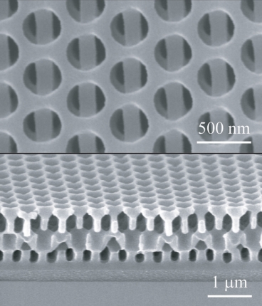 |
| The new 3D nanofabrication method makes it possible to manufacture complex multi-layered solids all in one step. In this example, seen in these Scanning Electron Microscope images, a view from above (at top) shows alternating layers containing round holes and long bars. As seen from the side (lower image), the alternating shapes repeat through several layers. Image: Chih-Hao Chang |
Abstract:
The making of three-dimensional nanostructured materials — ones that have distinctive shapes and structures at scales of a few billionths of a meter — has become a fertile area of research, producing materials that are useful for electronics, photonics, phononics and biomedical devices. But the methods of making such materials have been limited in the 3-D complexity they can produce. Now, an MIT team has found a way to produce more complicated structures by using a blend of current "top-down" and "bottom-up" approaches.
A new way to build nanostructures: Combining top-down and bottom-up approaches, new low-cost method could be a boon to research with a variety of applications.
Cambridge, MA | Posted on July 6th, 2011The work is described in a paper published in June in the journal Nano Letters, co-authored by postdoc Chih-Hao Chang; George Barbastathis, the Singapore Research Professor of Optics and Professor of Mechanical Engineering; and six MIT graduate students.
One approach to making three-dimensional nanostructures — a top-down approach — is called phase-shift lithography, in which a two-dimensional mask shapes the intensity of light shining onto a layer of photoresist material (in the same way a photographic negative controls the amount of light reaching different areas of a print). The photoresist is altered only in the areas reached by the light. However, this approach requires very precisely manufactured phase masks, which are expensive and time-consuming to make.
Another method — a bottom-up approach — is to use self-assembling colloidal nanoparticles that form themselves into certain energetically favorable close-packed arrangements. These can then be used as a mask for physical deposition methods, such as vapor deposition, or etching of the surface, to produce 2-D structures, just as a stencil can be used to control where paint reaches a surface. But these methods are slow and limited by defects that can form in the self-assembly process, so although they can be used for the fabrication of 3-D structures, this is made difficult because any defects propagate through the layers.
"We do a little bit of both," Chang says. "We took a chemist's method and added in a flavor of engineering."
The new method is a hybrid in which the self-assembled array is produced directly on a substrate material, performing the function of a mask for the lithography process. The individual nanoparticles that assemble on the surface each act as tiny lenses, focusing the beam into an intensity pattern determined by their arrangement on the surface. The method, the authors say in their paper, "can be implemented as a novel technique to fabricate complex 3-D nanostructures in all fields of nanoscale research."
Depending on the shapes and arrangements of the tiny glass beads they use for the self-assembly part of the process, it is possible to create a great variety of structures, "from holes to higher-density posts, rings, flowery structures, all using the exact same system," Chang says. "It's a very simple way to make 3-D nanostructures, and probably the cheapest way right now. You can use it for many things."
Team members, whose specialty is in optics, say the first structures they plan to make are photonic crystals, whose structure can manipulate the behavior of light beams passing through them. But the method can also be used to make phononic materials, which control waves of heat or sound, or even to make filters with precisely controlled porosity, which might have biomedical applications.
John Rogers SM '92, PhD '95, a professor of materials science and engineering and professor of chemistry at the University of Illinois at Urbana-Champaign who was not involved in this work, says these MIT researchers have found "a remarkably simple way to do a very hard thing in nanofabrication, i.e., to create large-scale, three-dimensional nanostructures with useful shapes."
Rogers says, "The experimental simplicity, and the resulting access to structures that would be difficult or impossible to achieve in other ways, suggest that the approach will be useful for many fields of application, ranging from photonic crystals to engineered filter membranes and others."
Written by David Chandler, MIT News Office
####
For more information, please click here
Contacts:
Marta Buczek
MIT News Office
617.253.2702
Copyright © MIT
If you have a comment, please Contact us.Issuers of news releases, not 7th Wave, Inc. or Nanotechnology Now, are solely responsible for the accuracy of the content.
Bookmark:


| Related News Press |
News and information
![]() Quantum computer improves AI predictions April 17th, 2026
Quantum computer improves AI predictions April 17th, 2026
![]() Flexible sensor gains sensitivity under pressure April 17th, 2026
Flexible sensor gains sensitivity under pressure April 17th, 2026
![]() A reusable chip for particulate matter sensing April 17th, 2026
A reusable chip for particulate matter sensing April 17th, 2026
![]() Detecting vibrational quantum beating in the predissociation dynamics of SF6 using time-resolved photoelectron spectroscopy April 17th, 2026
Detecting vibrational quantum beating in the predissociation dynamics of SF6 using time-resolved photoelectron spectroscopy April 17th, 2026
3D & 4D printing/Additive-manufacturing
![]() Presenting: Ultrasound-based printing of 3D materials—potentially inside the body December 8th, 2023
Presenting: Ultrasound-based printing of 3D materials—potentially inside the body December 8th, 2023
![]() Fiber sensing scientists invent 3D printed fiber microprobe for measuring in vivo biomechanical properties of tissue and even single cell February 10th, 2023
Fiber sensing scientists invent 3D printed fiber microprobe for measuring in vivo biomechanical properties of tissue and even single cell February 10th, 2023
![]() 3D-printed decoder, AI-enabled image compression could enable higher-res displays December 9th, 2022
3D-printed decoder, AI-enabled image compression could enable higher-res displays December 9th, 2022
![]() Researchers design new inks for 3D-printable wearable bioelectronics: Potential uses include printing electronic tattoos for medical tracking applications August 19th, 2022
Researchers design new inks for 3D-printable wearable bioelectronics: Potential uses include printing electronic tattoos for medical tracking applications August 19th, 2022
Chip Technology
![]() A reusable chip for particulate matter sensing April 17th, 2026
A reusable chip for particulate matter sensing April 17th, 2026
![]() Metasurfaces smooth light to boost magnetic sensing precision January 30th, 2026
Metasurfaces smooth light to boost magnetic sensing precision January 30th, 2026
Nanomedicine
![]() A fundamentally new therapeutic approach to cystic fibrosis: Nanobody repairs cellular defect April 17th, 2026
A fundamentally new therapeutic approach to cystic fibrosis: Nanobody repairs cellular defect April 17th, 2026
![]() New molecular technology targets tumors and simultaneously silences two ‘undruggable’ cancer genes August 8th, 2025
New molecular technology targets tumors and simultaneously silences two ‘undruggable’ cancer genes August 8th, 2025
![]() New imaging approach transforms study of bacterial biofilms August 8th, 2025
New imaging approach transforms study of bacterial biofilms August 8th, 2025
![]() Electrifying results shed light on graphene foam as a potential material for lab grown cartilage June 6th, 2025
Electrifying results shed light on graphene foam as a potential material for lab grown cartilage June 6th, 2025
Nanoelectronics
![]() Lab to industry: InSe wafer-scale breakthrough for future electronics August 8th, 2025
Lab to industry: InSe wafer-scale breakthrough for future electronics August 8th, 2025
![]() Interdisciplinary: Rice team tackles the future of semiconductors Multiferroics could be the key to ultralow-energy computing October 6th, 2023
Interdisciplinary: Rice team tackles the future of semiconductors Multiferroics could be the key to ultralow-energy computing October 6th, 2023
![]() Key element for a scalable quantum computer: Physicists from Forschungszentrum Jülich and RWTH Aachen University demonstrate electron transport on a quantum chip September 23rd, 2022
Key element for a scalable quantum computer: Physicists from Forschungszentrum Jülich and RWTH Aachen University demonstrate electron transport on a quantum chip September 23rd, 2022
![]() Reduced power consumption in semiconductor devices September 23rd, 2022
Reduced power consumption in semiconductor devices September 23rd, 2022
Discoveries
![]() Quantum computer improves AI predictions April 17th, 2026
Quantum computer improves AI predictions April 17th, 2026
![]() Flexible sensor gains sensitivity under pressure April 17th, 2026
Flexible sensor gains sensitivity under pressure April 17th, 2026
![]() A reusable chip for particulate matter sensing April 17th, 2026
A reusable chip for particulate matter sensing April 17th, 2026
![]() Detecting vibrational quantum beating in the predissociation dynamics of SF6 using time-resolved photoelectron spectroscopy April 17th, 2026
Detecting vibrational quantum beating in the predissociation dynamics of SF6 using time-resolved photoelectron spectroscopy April 17th, 2026
Materials/Metamaterials/Magnetoresistance
![]() First real-time observation of two-dimensional melting process: Researchers at Mainz University unveil new insights into magnetic vortex structures August 8th, 2025
First real-time observation of two-dimensional melting process: Researchers at Mainz University unveil new insights into magnetic vortex structures August 8th, 2025
![]() Researchers unveil a groundbreaking clay-based solution to capture carbon dioxide and combat climate change June 6th, 2025
Researchers unveil a groundbreaking clay-based solution to capture carbon dioxide and combat climate change June 6th, 2025
![]() A 1960s idea inspires NBI researchers to study hitherto inaccessible quantum states June 6th, 2025
A 1960s idea inspires NBI researchers to study hitherto inaccessible quantum states June 6th, 2025
![]() Institute for Nanoscience hosts annual proposal planning meeting May 16th, 2025
Institute for Nanoscience hosts annual proposal planning meeting May 16th, 2025
Announcements
![]() A fundamentally new therapeutic approach to cystic fibrosis: Nanobody repairs cellular defect April 17th, 2026
A fundamentally new therapeutic approach to cystic fibrosis: Nanobody repairs cellular defect April 17th, 2026
![]() UC Irvine physicists discover method to reverse ‘quantum scrambling’ : The work addresses the problem of information loss in quantum computing system April 17th, 2026
UC Irvine physicists discover method to reverse ‘quantum scrambling’ : The work addresses the problem of information loss in quantum computing system April 17th, 2026
Photonics/Optics/Lasers
![]() Metasurfaces smooth light to boost magnetic sensing precision January 30th, 2026
Metasurfaces smooth light to boost magnetic sensing precision January 30th, 2026
![]() From sensors to smart systems: the rise of AI-driven photonic noses January 30th, 2026
From sensors to smart systems: the rise of AI-driven photonic noses January 30th, 2026
|
|
||
|
|
||
| The latest news from around the world, FREE | ||
|
|
||
|
|
||
| Premium Products | ||
|
|
||
|
Only the news you want to read!
Learn More |
||
|
|
||
|
Full-service, expert consulting
Learn More |
||
|
|
||