Home > Press > Ultrathin Alternative to Silicon for Future Electronics
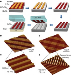 |
| Fabricating an indium oxide (InAs) device starts with a) epitaxially growing and etching InAs into nanoribbon arrays that are get stamped onto a silicon/silica (Si/SiO2 ) substrate; b) and c) InAs nanoribbon arrays on Si/SiO2; d) and e) InAs nanoribbon superstructures on Si/SiO2. |
Abstract:
Berkeley researchers have successfully used ultra-thin layers of the semiconductor indium arsenide to create a nanoscale transistor with excellent electronic properties. The technique could be applied to other III-V semiconductors as well for future high-speed, low-power electronic devices.
Ultrathin Alternative to Silicon for Future Electronics
Berkeley, CA | Posted on November 23rd, 2010There's good news in the search for the next generation of semiconductors. Researchers with the U.S. Department of Energy's Lawrence Berkeley National Laboratory (Berkeley Lab) and the University of California (UC) Berkeley, have successfully integrated ultra-thin layers of the semiconductor indium arsenide onto a silicon substrate to create a nanoscale transistor with excellent electronic properties. A member of the III-V family of semiconductors, indium arsenide offers several advantages as an alternative to silicon including superior electron mobility and velocity, which makes it an oustanding candidate for future high-speed, low-power electronic devices.
"We've shown a simple route for the heterogeneous integration of indium arsenide layers down to a thickness of 10 nanometers on silicon substrates," says Ali Javey, a faculty scientist in Berkeley Lab's Materials Sciences Division and a professor of electrical engineering and computer science at UC Berkeley, who led this research.
"The devices we subsequently fabricated were shown to operate near the projected performance limits of III-V devices with minimal leakage current. Our devices also exhibited superior performance in terms of current density and transconductance as compared to silicon transistors of similar dimensions."
For all its wondrous electronic properties, silicon has limitations that have prompted an intense search for alternative semiconductors to be used in future devices. Javey and his research group have focused on compound III-V semiconductors, which feature superb electron transport properties. The challenge has been to find a way of plugging these compound semiconductors into the well- established, low-cost processing technology used to produce today's silicon-based devices. Given the large lattice mismatch between silicon and III-V compound semiconductors, direct hetero-epitaxial growth of III-V on silicon substrates is challenging and complex, and often results in a high volume of defects.
"We've demonstrated what we are calling an �XOI,' or compound semiconductor-on-insulator technology platform, that is parallel to today's �SOI,' or silicon-on-insulator platform," says Javey. "Using an epitaxial transfer method, we transferred ultrathin layers of single-crystal indium- arsenide on silicon/silica substrates, then fabricated devices using conventional processing techniques in order to characterize the XOI material and device properties."
The results of this research have been published in the journal Nature, in a paper titled, "Ultrathin compound semiconductor on insulator layers for high-performance nanoscale transistors." Co-authoring the report with Javey were Hyunhyub Ko, Kuniharu Takei, Rehan Kapadia, Steven Chuang, Hui Fang, Paul Leu, Kartik Ganapathi, Elena Plis, Ha Sul Kim, Szu-Ying Chen, Morten Madsen, Alexandra Ford, Yu-Lun Chueh, Sanjay Krishna and Sayeef Salahuddin.
To make their XOI platforms, Javey and his collaborators grew single-crystal indium arsenide thin films (10 to 100 nanometers thick) on a preliminary source substrate then lithographically patterned the films into ordered arrays of nanoribbons. After being removed from the source substrate through a selective wet-etching of an underlying sacrificial layer, the nanoribbon arrays were transferred to the silicon/silica substrate via a stamping process.
Javey attributed the excellent electronic performance of the XOI transistors to the small dimensions of the active "X" layer and the critical role played by quantum confinement, which served to tune the material's band structure and transport properties. Although he and his group only used indium arsenide as their compound semiconductor, the technology should readily accommodate other compound III/V semiconductors as well.
"Future research on the scalability of our process for 8-inch and 12-inch wafer processing is needed," Javey said.
"Moving forward we believe that the XOI substrates can be obtained through a wafer bonding process, but our technique should make it possible to fabricate both p- and n- type transistors on the same chip for complementary electronics based on optimal III-V semiconductors.
"Furthermore, this concept can be used to directly integrate high performance photodiodes, lasers, and light emitting diodes on conventional silicon substrates. Uniquely, this technique could enable us to study the basic material properties of inorganic semiconductors when the thickness is scaled down to only a few atomic layers."
This research was funded in part by an LDRD grant from the Lawrence Berkeley National Laboratory, and by the MARCO/MSD Focus Center at MIT, the Intel Corporation and the Berkeley Sensor and Actuator Center.
For more about the research of Ali Javey, visit his Website at nano.eecs.berkeley.edu
####
About Berkeley Lab
Berkeley Lab is a U.S. Department of Energy national laboratory located in Berkeley, California. It conducts unclassified scientific research for DOE�s Office of Science and is managed by the University of California.
Visit our Website at www.lbl.gov
For more information, please click here
Contacts:
Lynn Yarris
(510) 486-5375
Copyright © Berkeley Lab
If you have a comment, please Contact us.Issuers of news releases, not 7th Wave, Inc. or Nanotechnology Now, are solely responsible for the accuracy of the content.
Bookmark:


| Related News Press |
News and information
![]() Quantum computer improves AI predictions April 17th, 2026
Quantum computer improves AI predictions April 17th, 2026
![]() Flexible sensor gains sensitivity under pressure April 17th, 2026
Flexible sensor gains sensitivity under pressure April 17th, 2026
![]() A reusable chip for particulate matter sensing April 17th, 2026
A reusable chip for particulate matter sensing April 17th, 2026
![]() Detecting vibrational quantum beating in the predissociation dynamics of SF6 using time-resolved photoelectron spectroscopy April 17th, 2026
Detecting vibrational quantum beating in the predissociation dynamics of SF6 using time-resolved photoelectron spectroscopy April 17th, 2026
Thin films
![]() Tiny nanosheets, big leap: A new sensor detects ethanol at ultra-low levels January 30th, 2026
Tiny nanosheets, big leap: A new sensor detects ethanol at ultra-low levels January 30th, 2026
![]() Utilizing palladium for addressing contact issues of buried oxide thin film transistors April 5th, 2024
Utilizing palladium for addressing contact issues of buried oxide thin film transistors April 5th, 2024
![]() Understanding the mechanism of non-uniform formation of diamond film on tools: Paving the way to a dry process with less environmental impact March 24th, 2023
Understanding the mechanism of non-uniform formation of diamond film on tools: Paving the way to a dry process with less environmental impact March 24th, 2023
![]() New study introduces the best graphite films: The work by Distinguished Professor Feng Ding at UNIST has been published in the October 2022 issue of Nature Nanotechnology November 4th, 2022
New study introduces the best graphite films: The work by Distinguished Professor Feng Ding at UNIST has been published in the October 2022 issue of Nature Nanotechnology November 4th, 2022
Govt.-Legislation/Regulation/Funding/Policy
![]() Quantum computer improves AI predictions April 17th, 2026
Quantum computer improves AI predictions April 17th, 2026
![]() Metasurfaces smooth light to boost magnetic sensing precision January 30th, 2026
Metasurfaces smooth light to boost magnetic sensing precision January 30th, 2026
![]() New imaging approach transforms study of bacterial biofilms August 8th, 2025
New imaging approach transforms study of bacterial biofilms August 8th, 2025
Possible Futures
![]() A fundamentally new therapeutic approach to cystic fibrosis: Nanobody repairs cellular defect April 17th, 2026
A fundamentally new therapeutic approach to cystic fibrosis: Nanobody repairs cellular defect April 17th, 2026
![]() UC Irvine physicists discover method to reverse �quantum scrambling� : The work addresses the problem of information loss in quantum computing system April 17th, 2026
UC Irvine physicists discover method to reverse �quantum scrambling� : The work addresses the problem of information loss in quantum computing system April 17th, 2026
Academic/Education
![]() Rice University launches Rice Synthetic Biology Institute to improve lives January 12th, 2024
Rice University launches Rice Synthetic Biology Institute to improve lives January 12th, 2024
![]() Multi-institution, $4.6 million NSF grant to fund nanotechnology training September 9th, 2022
Multi-institution, $4.6 million NSF grant to fund nanotechnology training September 9th, 2022
Chip Technology
![]() A reusable chip for particulate matter sensing April 17th, 2026
A reusable chip for particulate matter sensing April 17th, 2026
![]() Metasurfaces smooth light to boost magnetic sensing precision January 30th, 2026
Metasurfaces smooth light to boost magnetic sensing precision January 30th, 2026
Nanoelectronics
![]() Lab to industry: InSe wafer-scale breakthrough for future electronics August 8th, 2025
Lab to industry: InSe wafer-scale breakthrough for future electronics August 8th, 2025
![]() Interdisciplinary: Rice team tackles the future of semiconductors Multiferroics could be the key to ultralow-energy computing October 6th, 2023
Interdisciplinary: Rice team tackles the future of semiconductors Multiferroics could be the key to ultralow-energy computing October 6th, 2023
![]() Key element for a scalable quantum computer: Physicists from Forschungszentrum J�lich and RWTH Aachen University demonstrate electron transport on a quantum chip September 23rd, 2022
Key element for a scalable quantum computer: Physicists from Forschungszentrum J�lich and RWTH Aachen University demonstrate electron transport on a quantum chip September 23rd, 2022
![]() Reduced power consumption in semiconductor devices September 23rd, 2022
Reduced power consumption in semiconductor devices September 23rd, 2022
Announcements
![]() A fundamentally new therapeutic approach to cystic fibrosis: Nanobody repairs cellular defect April 17th, 2026
A fundamentally new therapeutic approach to cystic fibrosis: Nanobody repairs cellular defect April 17th, 2026
![]() UC Irvine physicists discover method to reverse �quantum scrambling� : The work addresses the problem of information loss in quantum computing system April 17th, 2026
UC Irvine physicists discover method to reverse �quantum scrambling� : The work addresses the problem of information loss in quantum computing system April 17th, 2026
Grants/Sponsored Research/Awards/Scholarships/Gifts/Contests/Honors/Records
![]() Quantum computer improves AI predictions April 17th, 2026
Quantum computer improves AI predictions April 17th, 2026
![]() Detecting vibrational quantum beating in the predissociation dynamics of SF6 using time-resolved photoelectron spectroscopy April 17th, 2026
Detecting vibrational quantum beating in the predissociation dynamics of SF6 using time-resolved photoelectron spectroscopy April 17th, 2026
![]() Metasurfaces smooth light to boost magnetic sensing precision January 30th, 2026
Metasurfaces smooth light to boost magnetic sensing precision January 30th, 2026
|
|
||
|
|
||
| The latest news from around the world, FREE | ||
|
|
||
|
|
||
| Premium Products | ||
|
|
||
|
Only the news you want to read!
Learn More |
||
|
|
||
|
Full-service, expert consulting
Learn More |
||
|
|
||