Home > Press > Record number of papers at SPIE Advanced Lithography conference reports imec’s progress in advanced lithography
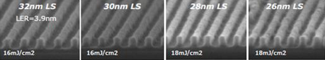 |
| EUV resists are steadily improving and now nicely resolve 27nm LS on the EUV ADT. |
Abstract:
At next week's SPIE Advanced Lithography Conference (www.spie.org) being held February 22 - 26 in San Jose, California, imec technologists will contribute a record number of over 30 papers showing their newest breakthroughs in advanced semiconductor lithography research.
While imec pushes 193nm to its limits by investigating cost-effective double patterning methods and by source mask optimization for 22nm half pitch, most research has been shifted to EUVL (extreme ultraviolet lithography). Today, EUV is the most promising cost-effective method for insertion at the 22nm node and approaches preproduction at imec by the end of 2010.
Record number of papers at SPIE Advanced Lithography conference reports imec’s progress in advanced lithography
Leuven, Belgium | Posted on February 16th, 2010EUV approaches preproduction at imec by end 2010
With the installation of Hamatech's MaskTrack Pro photomask cleaning system, imec is now ready to start its research on EUV mask cleaning. Pristine, defect-free masks at point-of-exposure have become a critical issue in the advancement of EUVL. Since EUV masks have no protecting pellicle, each time they are handled, a risk for extra defects due to particle formation exists. As the only research facility with a complete mask integrity infrastructure, imec will now start with some of its key core partners research on innovative mask cleaning technology to make sure that EUV masks are always clean before they are loaded into the scanner. Apart from contamination by particles, potential (photon-induced) organic contamination will also be studied. This unique research will enable to develop processes of record (PORs) for EUV mask cleaning, which will allow to accelerate total process development for yielding manufacturing based on EUV lithography.
Currently, imec is developing EUV process technology by applying ASML's EUV alpha demo tool (ADT); its successor, the EUV preproduction tool (ASML NXE:3100), is scheduled for installation in Q4 2010. Using the ADT, progress has been made on many aspects of EUV Lithography and preparation for the NXE:3100 is on-going.
And promising progress has been achieved in EUV resist performance. Imec now has resists to pattern 27nm features on the alpha demo tool and is confident that suitable resists for 22nm and later on 16nm are within reach on future exposure tools. A set-up to quantify resist outgassing became operational and is now used routinely in material screening and to qualify materials for ADT exposures.
Pushing 193nm lithography towards 22nm
Imec achieved major progress in the cost reduction of double patterning. Imec compares and evaluates chemicals and techniques for litho-process-litho-etch solutions as cost effective alternatives to the litho-etch-litho-etch process. By avoiding the etch step the process cost can be reduced. First results showed a litho-process-litho-etch solution as a viable process, in the first place for designs with a repeated, regular geometry, such as memory ICs. Today, resulting from a lot of research on intelligent design split, imec also reports that litho-process-litho-etch double patterning is a suitable and cost-effective technology for random logic application at 32nm half pitch. And very good critical dimension uniformity (CDU) of the first and second patterns has been measured down to 26nm half pitch.
Imec also started a program on source mask optimization including diffractive optical elements and flexible illuminators to further push 193nm to its limits. With source mask optimization, the illumination shape is tailored to the specific layout to be printed, improving in that way the resolution and process margins to some extent. These results show the potential to push 193nm lithography towards the 22nm node.
"I'm very proud that our lithography research team has achieved these amazing results over the last year. Thanks to their efforts and our unique infrastructure which we expand dependent on the technology needs, we are on track for cost-effective double patterning for the 32nm half pitch node and to introduce EUV at 22nm;" said Kurt Ronse, director advanced lithography program at imec.
####
About imec
Imec is a world-leading independent research center in nanoelectronics and nanotechnology.
Imec is headquartered in Leuven, Belgium, and has offices in Belgium, the Netherlands, Taiwan, US, China and Japan.
Its staff of more than 1,650 people include over 550 industrial residents and guest researchers. In 2008, imec's revenue (P&L) was 270 million euro.
For more information, please click here
Contacts:
imec: Katrien Marent
Director of External Communications
T: +32 16 28 18 80
Mobile : +32 474 30 28 66
Copyright © imec
If you have a comment, please Contact us.Issuers of news releases, not 7th Wave, Inc. or Nanotechnology Now, are solely responsible for the accuracy of the content.
Bookmark:


| Related News Press |
News and information
![]() Quantum computer improves AI predictions April 17th, 2026
Quantum computer improves AI predictions April 17th, 2026
![]() Flexible sensor gains sensitivity under pressure April 17th, 2026
Flexible sensor gains sensitivity under pressure April 17th, 2026
![]() A reusable chip for particulate matter sensing April 17th, 2026
A reusable chip for particulate matter sensing April 17th, 2026
![]() Detecting vibrational quantum beating in the predissociation dynamics of SF6 using time-resolved photoelectron spectroscopy April 17th, 2026
Detecting vibrational quantum beating in the predissociation dynamics of SF6 using time-resolved photoelectron spectroscopy April 17th, 2026
Chip Technology
![]() A reusable chip for particulate matter sensing April 17th, 2026
A reusable chip for particulate matter sensing April 17th, 2026
![]() Metasurfaces smooth light to boost magnetic sensing precision January 30th, 2026
Metasurfaces smooth light to boost magnetic sensing precision January 30th, 2026
Nanoelectronics
![]() Lab to industry: InSe wafer-scale breakthrough for future electronics August 8th, 2025
Lab to industry: InSe wafer-scale breakthrough for future electronics August 8th, 2025
![]() Interdisciplinary: Rice team tackles the future of semiconductors Multiferroics could be the key to ultralow-energy computing October 6th, 2023
Interdisciplinary: Rice team tackles the future of semiconductors Multiferroics could be the key to ultralow-energy computing October 6th, 2023
![]() Key element for a scalable quantum computer: Physicists from Forschungszentrum Jülich and RWTH Aachen University demonstrate electron transport on a quantum chip September 23rd, 2022
Key element for a scalable quantum computer: Physicists from Forschungszentrum Jülich and RWTH Aachen University demonstrate electron transport on a quantum chip September 23rd, 2022
![]() Reduced power consumption in semiconductor devices September 23rd, 2022
Reduced power consumption in semiconductor devices September 23rd, 2022
Announcements
![]() A fundamentally new therapeutic approach to cystic fibrosis: Nanobody repairs cellular defect April 17th, 2026
A fundamentally new therapeutic approach to cystic fibrosis: Nanobody repairs cellular defect April 17th, 2026
![]() UC Irvine physicists discover method to reverse ‘quantum scrambling’ : The work addresses the problem of information loss in quantum computing system April 17th, 2026
UC Irvine physicists discover method to reverse ‘quantum scrambling’ : The work addresses the problem of information loss in quantum computing system April 17th, 2026
Interviews/Book Reviews/Essays/Reports/Podcasts/Journals/White papers/Posters
![]() A fundamentally new therapeutic approach to cystic fibrosis: Nanobody repairs cellular defect April 17th, 2026
A fundamentally new therapeutic approach to cystic fibrosis: Nanobody repairs cellular defect April 17th, 2026
![]() UC Irvine physicists discover method to reverse ‘quantum scrambling’ : The work addresses the problem of information loss in quantum computing system April 17th, 2026
UC Irvine physicists discover method to reverse ‘quantum scrambling’ : The work addresses the problem of information loss in quantum computing system April 17th, 2026
Events/Classes
![]() Institute for Nanoscience hosts annual proposal planning meeting May 16th, 2025
Institute for Nanoscience hosts annual proposal planning meeting May 16th, 2025
![]() A New Blue: Mysterious origin of the ribbontail ray’s electric blue spots revealed July 5th, 2024
A New Blue: Mysterious origin of the ribbontail ray’s electric blue spots revealed July 5th, 2024
![]() Researchers demonstrate co-propagation of quantum and classical signals: Study shows that quantum encryption can be implemented in existing fiber networks January 20th, 2023
Researchers demonstrate co-propagation of quantum and classical signals: Study shows that quantum encryption can be implemented in existing fiber networks January 20th, 2023
|
|
||
|
|
||
| The latest news from around the world, FREE | ||
|
|
||
|
|
||
| Premium Products | ||
|
|
||
|
Only the news you want to read!
Learn More |
||
|
|
||
|
Full-service, expert consulting
Learn More |
||
|
|
||