Home > Press > Researchers use electron microscope to turn nanotube into tiny transistor
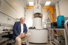 |
| Professor Dmitri Golberg has lead a time that used a unique tool inserted into an electron microscope to create a transistor that’s 25,000 smaller than the width of a human hair. CREDIT QUT |
Abstract:
An international team of researchers have used a unique tool inserted into an electron microscope to create a transistor that’s 25,000 times smaller than the width of a human hair.
Researchers use electron microscope to turn nanotube into tiny transistor
Brisbane, Australia | Posted on December 24th, 2021The research, published in the journal Science, involves researchers from Japan, China, Russia and Australia who have worked on the project that began five years ago.
QUT Centre for Materials Science co-director Professor Dmitri Golberg, who led the research project, said the result was a “very interesting fundamental discovery” which could lead a way for the future development of tiny transistors for future generations of advanced computing devices.
“In this work, we have shown it is possible to control the electronic properties of an individual carbon nanotube,” Professor Golberg said.
The researchers created the tiny transistor by simultaneously applying a force and low voltage which heated a carbon nanotube made up of few layers until outer tube shells separate, leaving just a single-layer nanotube.
The heat and strain then changed the “chilarity” of the nanotube, meaning the pattern in which the carbon atoms joined together to form the single-atomic layer of the nanotube wall was rearranged.
The result of the new structure connecting the carbon atoms was that the nanotube was transformed into a transistor.
Professor Golberg’s team members from the National University of Science and Technology in Moscow created a theory explaining the changes in the atomic structure and properties observed in the transistor.
Lead author Dr Dai-Ming Tang, from the International Centre for Materials Nanoarchitectonics in Japan, said the research had demonstrated the ability to manipulate the molecular properties of the nanotube to fabricated nanoscale electrical device.
Dr Tang began working on the project five years ago when Professor Golberg headed up the research group at this centre.
“Semiconducting carbon nanotubes are promising for fabricating energy-efficient nanotransistors to build beyond-silicon microprocessors,” Dr Tang said.
“However, it remains a great challenge to control the chirality of individual carbon nanotubes, which uniquely determines the atomic geometry and electronic structure.
“In this work, we designed and fabricated carbon nanotube intramolecular transistors by altering the local chirality of a metallic nanotube segment by heating and mechanical strain.”
Professor Golberg said the research in demonstrating the fundamental science in creating the tiny transistor was a promising step towards building beyond-silicon microprocessors.
Transistors, which are used to switch and amplify electronic signals, are often called the “building blocks” of all electronic devices, including computers. For example, Apple says the chip which powers the future iPhones contains 15 billion transistors.
The computer industry has been focussed on developing smaller and smaller transistors for decades, but faces the limitations of silicon.
In recent years, researchers have made significant steps in developing nanotransistors, which are so small that millions of them could fit onto the head of a pin.
“Miniaturization of transistors down to nanometer scale is a great challenge of the modern semiconducting industry and nanotechnology,” Professor Golberg said.
“The present discovery, although not practical for a mass-production of tiny transistors, shows a novel fabrication principle and opens up a new horizon of using thermomechanical treatments of nanotubes for obtaining the smallest transistors with desired characteristics.”
An international team of researchers have used a unique tool inserted into an electron microscope to create a transistor that’s 25,000 smaller than the width of a human hair.
The research, published in the journal Science, involves researchers from Japan, China, Russia and Australia who have worked on the project that began five years ago.
QUT Centre for Materials Science co-director Professor Dmitri Golberg, who led the research project, said the result was a “very interesting fundamental discovery” which could lead a way for the future development of tiny transistors for future generations of advanced computing devices.
“In this work, we have shown it is possible to control the electronic properties of an individual carbon nanotube,” Professor Golberg said.
The researchers created the tiny transistor by simultaneously applying a force and low voltage which heated a carbon nanotube made up of few layers until outer tube shells separate, leaving just a single-layer nanotube.
The heat and strain then changed the “chilarity” of the nanotube, meaning the pattern in which the carbon atoms joined together to form the single-atomic layer of the nanotube wall was rearranged.
The result of the new structure connecting the carbon atoms was that the nanotube was transformed into a transistor.
Professor Golberg’s team members from the National University of Science and Technology in Moscow created a theory explaining the changes in the atomic structure and properties observed in the transistor.
Lead author Dr Dai-Ming Tang, from the International Centre for Materials Nanoarchitectonics in Japan, said the research had demonstrated the ability to manipulate the molecular properties of the nanotube to fabricated nanoscale electrical device.
Dr Tang began working on the project five years ago when Professor Golberg headed up the research group at this centre.
“Semiconducting carbon nanotubes are promising for fabricating energy-efficient nanotransistors to build beyond-silicon microprocessors,” Dr Tang said.
“However, it remains a great challenge to control the chirality of individual carbon nanotubes, which uniquely determines the atomic geometry and electronic structure.
“In this work, we designed and fabricated carbon nanotube intramolecular transistors by altering the local chirality of a metallic nanotube segment by heating and mechanical strain.”
Professor Golberg said the research in demonstrating the fundamental science in creating the tiny transistor was a promising step towards building beyond-silicon microprocessors.
Transistors, which are used to switch and amplify electronic signals, are often called the “building blocks” of all electronic devices, including computers. For example, Apple says the chip which powers the future iPhones contains 15 billion transistors.
The computer industry has been focussed on developing smaller and smaller transistors for decades, but faces the limitations of silicon.
In recent years, researchers have made significant steps in developing nanotransistors, which are so small that millions of them could fit onto the head of a pin.
“Miniaturization of transistors down to nanometer scale is a great challenge of the modern semiconducting industry and nanotechnology,” Professor Golberg said.
“The present discovery, although not practical for a mass-production of tiny transistors, shows a novel fabrication principle and opens up a new horizon of using thermomechanical treatments of nanotubes for obtaining the smallest transistors with desired characteristics.”
####
For more information, please click here
Contacts:
Rod Chester
Queensland University of Technology
Office: 61-731-389-449
Copyright © Queensland University of Technology
If you have a comment, please Contact us.Issuers of news releases, not 7th Wave, Inc. or Nanotechnology Now, are solely responsible for the accuracy of the content.
Bookmark:


| Related Links |
| Related News Press |
News and information
![]() Simulating magnetization in a Heisenberg quantum spin chain April 5th, 2024
Simulating magnetization in a Heisenberg quantum spin chain April 5th, 2024
![]() NRL charters Navy’s quantum inertial navigation path to reduce drift April 5th, 2024
NRL charters Navy’s quantum inertial navigation path to reduce drift April 5th, 2024
![]() Discovery points path to flash-like memory for storing qubits: Rice find could hasten development of nonvolatile quantum memory April 5th, 2024
Discovery points path to flash-like memory for storing qubits: Rice find could hasten development of nonvolatile quantum memory April 5th, 2024
Imaging
![]() Nanoscale CL thermometry with lanthanide-doped heavy-metal oxide in TEM March 8th, 2024
Nanoscale CL thermometry with lanthanide-doped heavy-metal oxide in TEM March 8th, 2024
![]() The USTC realizes In situ electron paramagnetic resonance spectroscopy using single nanodiamond sensors November 3rd, 2023
The USTC realizes In situ electron paramagnetic resonance spectroscopy using single nanodiamond sensors November 3rd, 2023
![]() Observation of left and right at nanoscale with optical force October 6th, 2023
Observation of left and right at nanoscale with optical force October 6th, 2023
Possible Futures
![]() Discovery points path to flash-like memory for storing qubits: Rice find could hasten development of nonvolatile quantum memory April 5th, 2024
Discovery points path to flash-like memory for storing qubits: Rice find could hasten development of nonvolatile quantum memory April 5th, 2024
![]() With VECSELs towards the quantum internet Fraunhofer: IAF achieves record output power with VECSEL for quantum frequency converters April 5th, 2024
With VECSELs towards the quantum internet Fraunhofer: IAF achieves record output power with VECSEL for quantum frequency converters April 5th, 2024
Chip Technology
![]() Discovery points path to flash-like memory for storing qubits: Rice find could hasten development of nonvolatile quantum memory April 5th, 2024
Discovery points path to flash-like memory for storing qubits: Rice find could hasten development of nonvolatile quantum memory April 5th, 2024
![]() Utilizing palladium for addressing contact issues of buried oxide thin film transistors April 5th, 2024
Utilizing palladium for addressing contact issues of buried oxide thin film transistors April 5th, 2024
![]() HKUST researchers develop new integration technique for efficient coupling of III-V and silicon February 16th, 2024
HKUST researchers develop new integration technique for efficient coupling of III-V and silicon February 16th, 2024
Nanotubes/Buckyballs/Fullerenes/Nanorods/Nanostrings
![]() Tests find no free-standing nanotubes released from tire tread wear September 8th, 2023
Tests find no free-standing nanotubes released from tire tread wear September 8th, 2023
![]() Detection of bacteria and viruses with fluorescent nanotubes July 21st, 2023
Detection of bacteria and viruses with fluorescent nanotubes July 21st, 2023
Discoveries
![]() Chemical reactions can scramble quantum information as well as black holes April 5th, 2024
Chemical reactions can scramble quantum information as well as black holes April 5th, 2024
![]() New micromaterial releases nanoparticles that selectively destroy cancer cells April 5th, 2024
New micromaterial releases nanoparticles that selectively destroy cancer cells April 5th, 2024
![]() Utilizing palladium for addressing contact issues of buried oxide thin film transistors April 5th, 2024
Utilizing palladium for addressing contact issues of buried oxide thin film transistors April 5th, 2024
Announcements
![]() NRL charters Navy’s quantum inertial navigation path to reduce drift April 5th, 2024
NRL charters Navy’s quantum inertial navigation path to reduce drift April 5th, 2024
![]() Discovery points path to flash-like memory for storing qubits: Rice find could hasten development of nonvolatile quantum memory April 5th, 2024
Discovery points path to flash-like memory for storing qubits: Rice find could hasten development of nonvolatile quantum memory April 5th, 2024
Interviews/Book Reviews/Essays/Reports/Podcasts/Journals/White papers/Posters
![]() Simulating magnetization in a Heisenberg quantum spin chain April 5th, 2024
Simulating magnetization in a Heisenberg quantum spin chain April 5th, 2024
![]() Discovery points path to flash-like memory for storing qubits: Rice find could hasten development of nonvolatile quantum memory April 5th, 2024
Discovery points path to flash-like memory for storing qubits: Rice find could hasten development of nonvolatile quantum memory April 5th, 2024
Tools
![]() Ferroelectrically modulate the Fermi level of graphene oxide to enhance SERS response November 3rd, 2023
Ferroelectrically modulate the Fermi level of graphene oxide to enhance SERS response November 3rd, 2023
![]() The USTC realizes In situ electron paramagnetic resonance spectroscopy using single nanodiamond sensors November 3rd, 2023
The USTC realizes In situ electron paramagnetic resonance spectroscopy using single nanodiamond sensors November 3rd, 2023
|
|
||
|
|
||
| The latest news from around the world, FREE | ||
|
|
||
|
|
||
| Premium Products | ||
|
|
||
|
Only the news you want to read!
Learn More |
||
|
|
||
|
Full-service, expert consulting
Learn More |
||
|
|
||