Home > Press > Diamonds show promise for spintronic devices: New experiments demonstrate the potential for diamond as a material for spintronics
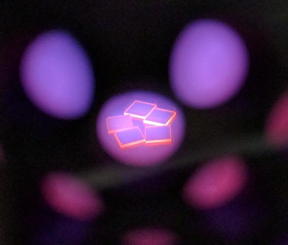 |
| Diamond plates undergoing surface termination treatment in a hydrogen plasma. CREDIT Daniel Creedon |
Abstract:
Conventional electronics rely on controlling electric charge. Recently, researchers have been exploring the potential for a new technology, called spintronics, that relies on detecting and controlling a particle's spin. This technology could lead to new types of more efficient and powerful devices.
Diamonds show promise for spintronic devices: New experiments demonstrate the potential for diamond as a material for spintronics
Washington, DC | Posted on January 30th, 2018In a paper published in Applied Physics Letters, from AIP Publishing, researchers measured how strongly a charge carrier's spin interacts with a magnetic field in diamond. This crucial property shows diamond as a promising material for spintronic devices.
Diamond is attractive because it would be easier to process and fabricate into spintronic devices than typical semiconductor materials, said Golrokh Akhgar, a physicist at La Trobe University in Australia. Conventional quantum devices are based on multiple thin layers of semiconductors, which require an elaborate fabrication process in an ultrahigh vacuum.
"Diamond is normally an extremely good insulator," Akhgar said. But, when exposed to hydrogen plasma, the diamond incorporates hydrogen atoms into its surface. When a hydrogenated diamond is introduced to moist air, it becomes electrically conductive because a thin layer of water forms on its surface, pulling electrons from the diamond. The missing electrons at the diamond surface behave like positively charged particles, called holes, making the surface conductive.
Researchers found that these holes have many of the right properties for spintronics. The most important property is a relativistic effect called spin-orbit coupling, where the spin of a charge carrier interacts with its orbital motion. A strong coupling enables researchers to control the particle's spin with an electric field.
In previous work, the researchers measured how strongly a hole's spin-orbit coupling could be engineered with an electric field. They also showed that an external electric field could tune the strength of the coupling.
In recent experiments, the researchers measured how strongly a hole's spin interacts with a magnetic field. For this measurement, the researchers applied constant magnetic fields of different strengths parallel to the diamond surface at temperatures below 4 Kelvin. They also simultaneously applied a steadily varying perpendicular field. By monitoring how the electrical resistance of the diamond changed, they determined the g-factor. This quantity could help researchers control spin in future devices using a magnetic field.
"The coupling strength of carrier spins to electric and magnetic fields lies at the heart of spintronics," Akhgar said. "We now have the two crucial parameters for the manipulation of spins in the conductive surface layer of diamond by either electric or magnetic fields."
Additionally, diamond is transparent, so it can be incorporated into optical devices that operate with visible or ultraviolet light. Nitrogen-vacancy diamonds -- which contain nitrogen atoms paired with missing carbon atoms in its crystal structure -- show promise as a quantum bit, or qubit, the basis for quantum information technology. Being able to manipulate spin and use it as a qubit could lead to yet more devices with untapped potential, Akhgar said.
####
For more information, please click here
Contacts:
Julia Majors
301-209-3090
Copyright © American Institute of Physics
If you have a comment, please Contact us.Issuers of news releases, not 7th Wave, Inc. or Nanotechnology Now, are solely responsible for the accuracy of the content.
Bookmark:


| Related Links |
| Related News Press |
News and information
![]() Quantum computer improves AI predictions April 17th, 2026
Quantum computer improves AI predictions April 17th, 2026
![]() Flexible sensor gains sensitivity under pressure April 17th, 2026
Flexible sensor gains sensitivity under pressure April 17th, 2026
![]() A reusable chip for particulate matter sensing April 17th, 2026
A reusable chip for particulate matter sensing April 17th, 2026
![]() Detecting vibrational quantum beating in the predissociation dynamics of SF6 using time-resolved photoelectron spectroscopy April 17th, 2026
Detecting vibrational quantum beating in the predissociation dynamics of SF6 using time-resolved photoelectron spectroscopy April 17th, 2026
2 Dimensional Materials
![]() Flexible sensor gains sensitivity under pressure April 17th, 2026
Flexible sensor gains sensitivity under pressure April 17th, 2026
Possible Futures
![]() A fundamentally new therapeutic approach to cystic fibrosis: Nanobody repairs cellular defect April 17th, 2026
A fundamentally new therapeutic approach to cystic fibrosis: Nanobody repairs cellular defect April 17th, 2026
![]() UC Irvine physicists discover method to reverse �quantum scrambling� : The work addresses the problem of information loss in quantum computing system April 17th, 2026
UC Irvine physicists discover method to reverse �quantum scrambling� : The work addresses the problem of information loss in quantum computing system April 17th, 2026
Spintronics
![]() Quantum materials: Electron spin measured for the first time June 9th, 2023
Quantum materials: Electron spin measured for the first time June 9th, 2023
Chip Technology
![]() A reusable chip for particulate matter sensing April 17th, 2026
A reusable chip for particulate matter sensing April 17th, 2026
![]() Metasurfaces smooth light to boost magnetic sensing precision January 30th, 2026
Metasurfaces smooth light to boost magnetic sensing precision January 30th, 2026
Quantum Computing
![]() Quantum computer improves AI predictions April 17th, 2026
Quantum computer improves AI predictions April 17th, 2026
![]() UC Irvine physicists discover method to reverse �quantum scrambling� : The work addresses the problem of information loss in quantum computing system April 17th, 2026
UC Irvine physicists discover method to reverse �quantum scrambling� : The work addresses the problem of information loss in quantum computing system April 17th, 2026
![]() Researchers develop molecular qubits that communicate at telecom frequencies October 3rd, 2025
Researchers develop molecular qubits that communicate at telecom frequencies October 3rd, 2025
Discoveries
![]() Quantum computer improves AI predictions April 17th, 2026
Quantum computer improves AI predictions April 17th, 2026
![]() Flexible sensor gains sensitivity under pressure April 17th, 2026
Flexible sensor gains sensitivity under pressure April 17th, 2026
![]() A reusable chip for particulate matter sensing April 17th, 2026
A reusable chip for particulate matter sensing April 17th, 2026
![]() Detecting vibrational quantum beating in the predissociation dynamics of SF6 using time-resolved photoelectron spectroscopy April 17th, 2026
Detecting vibrational quantum beating in the predissociation dynamics of SF6 using time-resolved photoelectron spectroscopy April 17th, 2026
Materials/Metamaterials/Magnetoresistance
![]() First real-time observation of two-dimensional melting process: Researchers at Mainz University unveil new insights into magnetic vortex structures August 8th, 2025
First real-time observation of two-dimensional melting process: Researchers at Mainz University unveil new insights into magnetic vortex structures August 8th, 2025
![]() Researchers unveil a groundbreaking clay-based solution to capture carbon dioxide and combat climate change June 6th, 2025
Researchers unveil a groundbreaking clay-based solution to capture carbon dioxide and combat climate change June 6th, 2025
![]() A 1960s idea inspires NBI researchers to study hitherto inaccessible quantum states June 6th, 2025
A 1960s idea inspires NBI researchers to study hitherto inaccessible quantum states June 6th, 2025
![]() Institute for Nanoscience hosts annual proposal planning meeting May 16th, 2025
Institute for Nanoscience hosts annual proposal planning meeting May 16th, 2025
Announcements
![]() A fundamentally new therapeutic approach to cystic fibrosis: Nanobody repairs cellular defect April 17th, 2026
A fundamentally new therapeutic approach to cystic fibrosis: Nanobody repairs cellular defect April 17th, 2026
![]() UC Irvine physicists discover method to reverse �quantum scrambling� : The work addresses the problem of information loss in quantum computing system April 17th, 2026
UC Irvine physicists discover method to reverse �quantum scrambling� : The work addresses the problem of information loss in quantum computing system April 17th, 2026
Interviews/Book Reviews/Essays/Reports/Podcasts/Journals/White papers/Posters
![]() A fundamentally new therapeutic approach to cystic fibrosis: Nanobody repairs cellular defect April 17th, 2026
A fundamentally new therapeutic approach to cystic fibrosis: Nanobody repairs cellular defect April 17th, 2026
![]() UC Irvine physicists discover method to reverse �quantum scrambling� : The work addresses the problem of information loss in quantum computing system April 17th, 2026
UC Irvine physicists discover method to reverse �quantum scrambling� : The work addresses the problem of information loss in quantum computing system April 17th, 2026
|
|
||
|
|
||
| The latest news from around the world, FREE | ||
|
|
||
|
|
||
| Premium Products | ||
|
|
||
|
Only the news you want to read!
Learn More |
||
|
|
||
|
Full-service, expert consulting
Learn More |
||
|
|
||