Home > Press > Application of air-sensitive semiconductors in nanoelectronics: 2-D semiconductor gallium selenide in encapsulated nanoelectronic devices
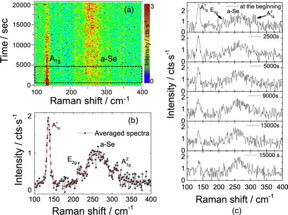 |
| Raman spectrum of 8 L GaSe taken at two different times during time evolution map. (a) Red dashed line is drawn as the guide for the eye. The constant intensity ratio of of ${{{A}}^{1}}_{1{\rm{g}}}$ and a-Se peaks indicates that oxidation stops approximately after 16 500 s. Thickness dependent Raman spectrum of GaSe for oxidation investigation. (b) Each spectrum was taken with 700 s � 3 of accumulation time. CREDIT Tomsk Polytechnic University |
Abstract:
A research group consisting of scientists from Tomsk Polytechnic University, Germany and Venezuela proved vulnerability of a two-dimensional semiconductor gallium selenide in air. This discovery will allow manufacturing superconducting nanoelectronics based on gallium selenide, which has never been previously achieved by any research team in the world.
Application of air-sensitive semiconductors in nanoelectronics: 2-D semiconductor gallium selenide in encapsulated nanoelectronic devices
Tomsk, Russia | Posted on September 22nd, 2017The study was published in Semiconductor Science and Technology.
One of the promising areas of modern materials science is the study of two-dimensional (2D) materials, i.e. thin films consisting of one or several atomic layers. 2D materials due to their electrical superconductivity and strength could be a basis for modern nanoelectronics. Optic applications in nanoelectronics require advanced materials capable of 'generating' great electron fluxes upon light irradiation. Gallium selenide (GaSe) is one of the 2D semiconductors that can cope with this problem most efficiently.
'Some research teams abroad tried to create electronic devices based on GaSe. However, despite extensive theoretical studies of this material, which were published in major scientific journals, the stability of the material in real devices remained unclear,' says Prof. Raul Rodriguez, the Department of Lasers and Lighting Engineering.
The research team revealed the reasons behind this. They studied GaSe by means of Raman spectroscopy and x-ray photoelectron spectroscopy that allowed proving the existence of chemical bonds between gallium and oxygen. Photoluminescence in oxidized substance is absent that also proves the formation of oxides. It means that the scientists revealed that GaSe oxidizes quickly in air and loses its electrical conductivity necessary for creating nanoeletronic devices.
'GaSe monolayers become oxidized almost immediately after being exposed to air. Further research of GASe stability in air will allow making proposals how to protect it and maintain its optoelectronic properties,' emphasize the authors.
According to Prof. Rodriguez, for GaSe not to lose its unique properties it should be placed in a vacuum or inert environment. For example, it can be applied in encapsulated devices that are vacuum-manufactured and then covered with a protective layer eliminating air penetration.
This method can be used to produce next generation optoelectronics, detectors, light sources and solar batteries. Such devices of ultra-small sizes will have very high quantum efficiency, i.e. they will be able to generate large electron fluxes under small external exposure.
####
For more information, please click here
Contacts:
Kristina Nabokova
382-270-5685
Copyright © Tomsk Polytechnic University
If you have a comment, please Contact us.Issuers of news releases, not 7th Wave, Inc. or Nanotechnology Now, are solely responsible for the accuracy of the content.
Bookmark:


| Related Links |
| Related News Press |
News and information
![]() Quantum computer improves AI predictions April 17th, 2026
Quantum computer improves AI predictions April 17th, 2026
![]() Flexible sensor gains sensitivity under pressure April 17th, 2026
Flexible sensor gains sensitivity under pressure April 17th, 2026
![]() A reusable chip for particulate matter sensing April 17th, 2026
A reusable chip for particulate matter sensing April 17th, 2026
![]() Detecting vibrational quantum beating in the predissociation dynamics of SF6 using time-resolved photoelectron spectroscopy April 17th, 2026
Detecting vibrational quantum beating in the predissociation dynamics of SF6 using time-resolved photoelectron spectroscopy April 17th, 2026
2 Dimensional Materials
![]() Flexible sensor gains sensitivity under pressure April 17th, 2026
Flexible sensor gains sensitivity under pressure April 17th, 2026
Hardware
![]() The present and future of computing get a boost from new research July 21st, 2023
The present and future of computing get a boost from new research July 21st, 2023
![]() A Carbon Nanotube Microprocessor Mature Enough to Say Hello: Three new breakthroughs make commercial nanotube processors possible March 2nd, 2020
A Carbon Nanotube Microprocessor Mature Enough to Say Hello: Three new breakthroughs make commercial nanotube processors possible March 2nd, 2020
![]() Powering the future: Smallest all-digital circuit opens doors to 5 nm next-gen semiconductor February 11th, 2020
Powering the future: Smallest all-digital circuit opens doors to 5 nm next-gen semiconductor February 11th, 2020
Possible Futures
![]() A fundamentally new therapeutic approach to cystic fibrosis: Nanobody repairs cellular defect April 17th, 2026
A fundamentally new therapeutic approach to cystic fibrosis: Nanobody repairs cellular defect April 17th, 2026
![]() UC Irvine physicists discover method to reverse �quantum scrambling� : The work addresses the problem of information loss in quantum computing system April 17th, 2026
UC Irvine physicists discover method to reverse �quantum scrambling� : The work addresses the problem of information loss in quantum computing system April 17th, 2026
Chip Technology
![]() A reusable chip for particulate matter sensing April 17th, 2026
A reusable chip for particulate matter sensing April 17th, 2026
![]() Metasurfaces smooth light to boost magnetic sensing precision January 30th, 2026
Metasurfaces smooth light to boost magnetic sensing precision January 30th, 2026
Optical computing/Photonic computing
![]() ICFO researchers overcome long-standing bottleneck in single photon detection with twisted 2D materials August 8th, 2025
ICFO researchers overcome long-standing bottleneck in single photon detection with twisted 2D materials August 8th, 2025
![]() Programmable electron-induced color router array May 14th, 2025
Programmable electron-induced color router array May 14th, 2025
Nanoelectronics
![]() Lab to industry: InSe wafer-scale breakthrough for future electronics August 8th, 2025
Lab to industry: InSe wafer-scale breakthrough for future electronics August 8th, 2025
![]() Interdisciplinary: Rice team tackles the future of semiconductors Multiferroics could be the key to ultralow-energy computing October 6th, 2023
Interdisciplinary: Rice team tackles the future of semiconductors Multiferroics could be the key to ultralow-energy computing October 6th, 2023
![]() Key element for a scalable quantum computer: Physicists from Forschungszentrum J�lich and RWTH Aachen University demonstrate electron transport on a quantum chip September 23rd, 2022
Key element for a scalable quantum computer: Physicists from Forschungszentrum J�lich and RWTH Aachen University demonstrate electron transport on a quantum chip September 23rd, 2022
![]() Reduced power consumption in semiconductor devices September 23rd, 2022
Reduced power consumption in semiconductor devices September 23rd, 2022
Discoveries
![]() Quantum computer improves AI predictions April 17th, 2026
Quantum computer improves AI predictions April 17th, 2026
![]() Flexible sensor gains sensitivity under pressure April 17th, 2026
Flexible sensor gains sensitivity under pressure April 17th, 2026
![]() A reusable chip for particulate matter sensing April 17th, 2026
A reusable chip for particulate matter sensing April 17th, 2026
![]() Detecting vibrational quantum beating in the predissociation dynamics of SF6 using time-resolved photoelectron spectroscopy April 17th, 2026
Detecting vibrational quantum beating in the predissociation dynamics of SF6 using time-resolved photoelectron spectroscopy April 17th, 2026
Announcements
![]() A fundamentally new therapeutic approach to cystic fibrosis: Nanobody repairs cellular defect April 17th, 2026
A fundamentally new therapeutic approach to cystic fibrosis: Nanobody repairs cellular defect April 17th, 2026
![]() UC Irvine physicists discover method to reverse �quantum scrambling� : The work addresses the problem of information loss in quantum computing system April 17th, 2026
UC Irvine physicists discover method to reverse �quantum scrambling� : The work addresses the problem of information loss in quantum computing system April 17th, 2026
Interviews/Book Reviews/Essays/Reports/Podcasts/Journals/White papers/Posters
![]() A fundamentally new therapeutic approach to cystic fibrosis: Nanobody repairs cellular defect April 17th, 2026
A fundamentally new therapeutic approach to cystic fibrosis: Nanobody repairs cellular defect April 17th, 2026
![]() UC Irvine physicists discover method to reverse �quantum scrambling� : The work addresses the problem of information loss in quantum computing system April 17th, 2026
UC Irvine physicists discover method to reverse �quantum scrambling� : The work addresses the problem of information loss in quantum computing system April 17th, 2026
Photonics/Optics/Lasers
![]() Metasurfaces smooth light to boost magnetic sensing precision January 30th, 2026
Metasurfaces smooth light to boost magnetic sensing precision January 30th, 2026
![]() From sensors to smart systems: the rise of AI-driven photonic noses January 30th, 2026
From sensors to smart systems: the rise of AI-driven photonic noses January 30th, 2026
|
|
||
|
|
||
| The latest news from around the world, FREE | ||
|
|
||
|
|
||
| Premium Products | ||
|
|
||
|
Only the news you want to read!
Learn More |
||
|
|
||
|
Full-service, expert consulting
Learn More |
||
|
|
||