Home > Press > Simultaneous Design and Nanomanufacturing Speeds Up Fabrication: Method enhances broadband light absorption in solar cells
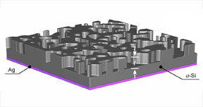 |
| A schematic of quasi-random nanowrinkles on the surface of a silicon wafer. |
Abstract:
Design and nanomanufacturing have collided inside a Northwestern University laboratory.
Simultaneous Design and Nanomanufacturing Speeds Up Fabrication: Method enhances broadband light absorption in solar cells
Evanston, IL | Posted on August 5th, 2017An interdisciplinary team of researchers has used mathematics and machine learning to design an optimal material for light management in solar cells and then fabricated the nanostructured surfaces simultaneously with a new nanomanufacturing technique.
�We have bridged the gap between design and nanomanufacturing,� said Wei Chen, the Wilson-Cook Professor in Engineering Design and professor of mechanical engineering in Northwestern�s McCormick School of Engineering, who led the study�s design component. �Instead of designing a structure element by element, we are now designing and optimizing it with a simple mathematic function and fabricating it at the same time.�
The fast, highly scalable, streamlined method could replace cumbersome trial-and-error nanomanufacturing and design methods, which often take vast resources to complete.
�The concurrent design and processing of nanostructures paves the way to avoid trial-and-error manufacturing, increasing the cost-effectiveness to prototype nanophotonic devices,� said Teri Odom, Charles E. and Emma H. Morrison Professor of Chemistry in Northwestern�s Weinberg College of Arts and Sciences and leader of the study�s nanofabrication component.
Researchers are currently interested in nanophotonic materials for light absorption in ultra-thin, flexible solar cells. The same principle could also be applied to implement color into clothing without dyes and to create anti-wet surfaces. For solar cells, the ideal nanostructure surface features quasi-random structures -- meaning the structures appear random but do have a pattern. Designing these patterns can be difficult and time consuming, since there are thousands of geometric variables that must be optimized simultaneously to discover the optimal surface pattern to absorb the most light.
�It is a very tedious job to fabricate the optimal design,� Chen said. �You could use nano-lithography, which is similar to 3-D printing, but it takes days and thousands of dollars just to print a little square. That�s not practical.�
To bypass the issues of nano-lithography, Odom and Chen manufactured the quasi-random structures with wrinkle lithography, a new nanomanufacturing technique that can rapidly transfer wrinkle patterns into different materials to realize a nearly unlimited number of quasi-random nanostructures. Formed by applying strain to a substrate, wrinkling is a simple method for the scalable fabrication of nanoscale surface structures.
�Importantly, the complex geometries can be described computationally with only three parameters -- instead of thousands typically required by other approaches,� Odom said. �We then used the digital designs in an iterative search loop to determine the optimal nanowrinkles for a desired outcome.�
Supported by the National Science Foundation and Office of Naval Research, the research was published online this week in the Proceedings of the National Academy of Sciences. Won-Kyu Lee, a Ph.D. student in Odom�s laboratory, served as the paper�s first author. Shuangcheng Yu, a Ph.D. student who recently graduated from Chen�s Integrated Design Automation Laboratory (IDEAL), served as the paper�s second author. Lee and Yu contributed equally to the work.
The team demonstrated the concurrent design and manufacturing method to fabricate 3-D photonic nanostructures on a silicon wafer for potential use as a solar cell. The resulting material absorbed 160 percent more light in the 800- to 1,200-nanometer wavelength -- a range in which current solar cells are inefficient -- than other designs.
�Light wavelengths have different frequencies, and we did not design for just one frequency,� Chen said. �We designed for the whole spectrum of sunlight frequencies, so the solar cell can absorb light over broadband wavelengths and over a wide collection of angles.�
Next, the team plans to apply its method to other materials, such as polymers, metals and oxides, for other photonics applications.
####
For more information, please click here
Contacts:
Megan Fellman
847-491-3115
Copyright © Northwestern University
If you have a comment, please Contact us.Issuers of news releases, not 7th Wave, Inc. or Nanotechnology Now, are solely responsible for the accuracy of the content.
Bookmark:


| Related Links |
| Related News Press |
News and information
![]() Decoding hydrogen‑bond network of electrolyte for cryogenic durable aqueous zinc‑ion batteries January 30th, 2026
Decoding hydrogen‑bond network of electrolyte for cryogenic durable aqueous zinc‑ion batteries January 30th, 2026
![]() COF scaffold membrane with gate‑lane nanostructure for efficient Li+/Mg2+ separation January 30th, 2026
COF scaffold membrane with gate‑lane nanostructure for efficient Li+/Mg2+ separation January 30th, 2026
Possible Futures
![]() Decoding hydrogen‑bond network of electrolyte for cryogenic durable aqueous zinc‑ion batteries January 30th, 2026
Decoding hydrogen‑bond network of electrolyte for cryogenic durable aqueous zinc‑ion batteries January 30th, 2026
![]() COF scaffold membrane with gate‑lane nanostructure for efficient Li+/Mg2+ separation January 30th, 2026
COF scaffold membrane with gate‑lane nanostructure for efficient Li+/Mg2+ separation January 30th, 2026
Discoveries
![]() From sensors to smart systems: the rise of AI-driven photonic noses January 30th, 2026
From sensors to smart systems: the rise of AI-driven photonic noses January 30th, 2026
![]() Decoding hydrogen‑bond network of electrolyte for cryogenic durable aqueous zinc‑ion batteries January 30th, 2026
Decoding hydrogen‑bond network of electrolyte for cryogenic durable aqueous zinc‑ion batteries January 30th, 2026
![]() COF scaffold membrane with gate‑lane nanostructure for efficient Li+/Mg2+ separation January 30th, 2026
COF scaffold membrane with gate‑lane nanostructure for efficient Li+/Mg2+ separation January 30th, 2026
Announcements
![]() Decoding hydrogen‑bond network of electrolyte for cryogenic durable aqueous zinc‑ion batteries January 30th, 2026
Decoding hydrogen‑bond network of electrolyte for cryogenic durable aqueous zinc‑ion batteries January 30th, 2026
![]() COF scaffold membrane with gate‑lane nanostructure for efficient Li+/Mg2+ separation January 30th, 2026
COF scaffold membrane with gate‑lane nanostructure for efficient Li+/Mg2+ separation January 30th, 2026
Interviews/Book Reviews/Essays/Reports/Podcasts/Journals/White papers/Posters
![]() Metasurfaces smooth light to boost magnetic sensing precision January 30th, 2026
Metasurfaces smooth light to boost magnetic sensing precision January 30th, 2026
![]() COF scaffold membrane with gate‑lane nanostructure for efficient Li+/Mg2+ separation January 30th, 2026
COF scaffold membrane with gate‑lane nanostructure for efficient Li+/Mg2+ separation January 30th, 2026
Energy
![]() Sensors innovations for smart lithium-based batteries: advancements, opportunities, and potential challenges August 8th, 2025
Sensors innovations for smart lithium-based batteries: advancements, opportunities, and potential challenges August 8th, 2025
![]() Simple algorithm paired with standard imaging tool could predict failure in lithium metal batteries August 8th, 2025
Simple algorithm paired with standard imaging tool could predict failure in lithium metal batteries August 8th, 2025
Photonics/Optics/Lasers
![]() Metasurfaces smooth light to boost magnetic sensing precision January 30th, 2026
Metasurfaces smooth light to boost magnetic sensing precision January 30th, 2026
![]() From sensors to smart systems: the rise of AI-driven photonic noses January 30th, 2026
From sensors to smart systems: the rise of AI-driven photonic noses January 30th, 2026
![]() ICFO researchers overcome long-standing bottleneck in single photon detection with twisted 2D materials August 8th, 2025
ICFO researchers overcome long-standing bottleneck in single photon detection with twisted 2D materials August 8th, 2025
Solar/Photovoltaic
![]() Spinel-type sulfide semiconductors to operate the next-generation LEDs and solar cells For solar-cell absorbers and green-LED source October 3rd, 2025
Spinel-type sulfide semiconductors to operate the next-generation LEDs and solar cells For solar-cell absorbers and green-LED source October 3rd, 2025
![]() KAIST researchers introduce new and improved, next-generation perovskite solar cell November 8th, 2024
KAIST researchers introduce new and improved, next-generation perovskite solar cell November 8th, 2024
![]() Groundbreaking precision in single-molecule optoelectronics August 16th, 2024
Groundbreaking precision in single-molecule optoelectronics August 16th, 2024
![]() Development of zinc oxide nanopagoda array photoelectrode: photoelectrochemical water-splitting hydrogen production January 12th, 2024
Development of zinc oxide nanopagoda array photoelectrode: photoelectrochemical water-splitting hydrogen production January 12th, 2024
Printing/Lithography/Inkjet/Inks/Bio-printing/Dyes
![]() Presenting: Ultrasound-based printing of 3D materials�potentially inside the body December 8th, 2023
Presenting: Ultrasound-based printing of 3D materials�potentially inside the body December 8th, 2023
![]() Simple ballpoint pen can write custom LEDs August 11th, 2023
Simple ballpoint pen can write custom LEDs August 11th, 2023
![]() Disposable electronics on a simple sheet of paper October 7th, 2022
Disposable electronics on a simple sheet of paper October 7th, 2022
|
|
||
|
|
||
| The latest news from around the world, FREE | ||
|
|
||
|
|
||
| Premium Products | ||
|
|
||
|
Only the news you want to read!
Learn More |
||
|
|
||
|
Full-service, expert consulting
Learn More |
||
|
|
||