Home > Press > Channeling valleytronics in graphene: Berkeley Lab researchers discover 1-D conducting channels in bilayer graphene
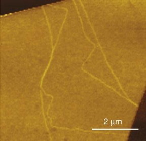 |
| In this near-field infrared nanoscopy image of bilayer graphene, domain walls are revealed by bright lines that arise because of the walls' local electronic structures and IR responses. CREDIT: Image courtesy of Feng Wang, Berkeley Lab |
Abstract:
To the list of potential applications of graphene - a two-dimensional semiconductor of pure carbon that is stronger and much faster than silicon - we can now add valleytronics, the coding of data in the wavelike motion of electrons as they speed through a conductor. Berkeley Lab researchers have discovered topologically protected one-dimensional electron conducting channels at the domain walls of bilayer graphene. These conducting channels are "valley polarized," which means they can serve as filters for electron valley polarization in future devices such as quantum computers.
Channeling valleytronics in graphene: Berkeley Lab researchers discover 1-D conducting channels in bilayer graphene
Berkeley, CA | Posted on May 6th, 2015"Combining near-field infrared nanometer-scale microscopy and low-temperature electrical transport measurements, we have recorded the first experimental observations of 1D ballistic electron conducting channels at bilayer graphene domain walls," says Feng Wang, a condensed matter physicist with Berkeley Lab's Materials Sciences Division, who led this work. "These 1D valley-polarized conducting channels featured a ballistic length of about 400 nanometers at 4 kelvin. Their existence opens up opportunities for exploring unique topological phases and valley physics in graphene."
Wang, who also holds an appointment with the University of California (UC) Berkeley Physics Department and is a member of the Kavli Energy NanoScience Institute (Kavli-ENSI), is the corresponding author of a paper describing this research in the journal Nature. The lead authors of the paper are Long Ju and Zhiwen Shi, members of Wang's research group. (See here for full list of authors.)
Valleytronics is generating a lot of excitement in the high-tech industry as a potential avenue to quantum computing. Like spintronics, valleytronics offers a tremendous advantage in data processing speeds over the electrical charge used in classical electronics.
"In valleytronics, electrons move through the lattice of a 2D semiconductor as a wave with two energy valleys, each valley being characterized by a distinct momentum and quantum valley number," Wang says. "This quantum valley number can be used to encode information when the electrons are in a minimum energy valley."
Recent theoretical work suggested that domain walls between AB- and BA-stacked bilayer graphene could provide an attractive place to realize one-dimensional electron conducting channels for valleytronics because the smoothness of the domain walls preserves electron valleys, unlike the atomic defects at graphene edges that result in valley-mixing. Until now, however, there has been no experimental evidence of these channels.
Working at Berkeley Lab's Advanced Light Source (ALS), a DOE Office of Science User Facility, Wang, Ju, Shi and their colleagues used tightly focused beams of infrared light to image in situ bilayer graphene layer-stacking domain walls on device substrates. Field effect devices fabricated over these domain walls revealed the 1D conducting channels.
In the bilayer graphene imaging work by Feng Wang and his group, IR light (yellow) is focused onto the apex of a metal-coated AFM tip and the backscattered infrared radiation is collected and measured.
"The infrared measurements were carried out at ALS beamline 5.4," says Shi. "The near-field infrared capabilities of this beamline enable optical spectroscopy with spatial resolutions that are way beyond the diffraction limit, allowing us to image the nanometer-wide domain walls in bilayer graphene."
Adds Ju, "That we were able to image the domain walls with a technique that is compatible with device fabrication was key to our work. With near-field IR spectroscopy, we could directly fabricate field effect devices over the domain walls and detect the 1D conducting channels."
To date, most valleytronics research has focused on the 2D semiconductors known as MX2 materials, which consist of a single layer of transition metal atoms, such as molybdenum or tungsten, sandwiched between two layers of chalcogen atoms, such as sulfur. The results of this study demonstrate that protected topological phases can also be realized in bilayer graphene, which is a tunable semiconductor, making the 2D carbon sheets useful for valleytronic applications.
"Our next step is to increase the ballistic length of these 1D channels so we can utilize them as electron valley filters, as well as for other manipulations of electron valleys in graphene," Wang says.
###
This research was primarily funded by the DOE Office of Science.
####
About DOE/Lawrence Berkeley National Laboratory
Lawrence Berkeley National Laboratory addresses the world's most urgent scientific challenges by advancing sustainable energy, protecting human health, creating new materials, and revealing the origin and fate of the universe. Founded in 1931, Berkeley Lab's scientific expertise has been recognized with 13 Nobel prizes. The University of California manages Berkeley Lab for the U.S. Department of Energy's Office of Science.
For more information, please click here
Contacts:
Lynn Yarris
510-486-5375
Copyright © DOE/Lawrence Berkeley National Laboratory
If you have a comment, please Contact us.Issuers of news releases, not 7th Wave, Inc. or Nanotechnology Now, are solely responsible for the accuracy of the content.
Bookmark:


| Related News Press |
News and information
![]() Quantum computer improves AI predictions April 17th, 2026
Quantum computer improves AI predictions April 17th, 2026
![]() Flexible sensor gains sensitivity under pressure April 17th, 2026
Flexible sensor gains sensitivity under pressure April 17th, 2026
![]() A reusable chip for particulate matter sensing April 17th, 2026
A reusable chip for particulate matter sensing April 17th, 2026
![]() Detecting vibrational quantum beating in the predissociation dynamics of SF6 using time-resolved photoelectron spectroscopy April 17th, 2026
Detecting vibrational quantum beating in the predissociation dynamics of SF6 using time-resolved photoelectron spectroscopy April 17th, 2026
Imaging
![]() Simple algorithm paired with standard imaging tool could predict failure in lithium metal batteries August 8th, 2025
Simple algorithm paired with standard imaging tool could predict failure in lithium metal batteries August 8th, 2025
![]() First real-time observation of two-dimensional melting process: Researchers at Mainz University unveil new insights into magnetic vortex structures August 8th, 2025
First real-time observation of two-dimensional melting process: Researchers at Mainz University unveil new insights into magnetic vortex structures August 8th, 2025
![]() New imaging approach transforms study of bacterial biofilms August 8th, 2025
New imaging approach transforms study of bacterial biofilms August 8th, 2025
Physics
![]() UC Irvine physicists discover method to reverse �quantum scrambling� : The work addresses the problem of information loss in quantum computing system April 17th, 2026
UC Irvine physicists discover method to reverse �quantum scrambling� : The work addresses the problem of information loss in quantum computing system April 17th, 2026
![]() Quantum computers simulate fundamental physics: shedding light on the building blocks of nature June 6th, 2025
Quantum computers simulate fundamental physics: shedding light on the building blocks of nature June 6th, 2025
![]() A 1960s idea inspires NBI researchers to study hitherto inaccessible quantum states June 6th, 2025
A 1960s idea inspires NBI researchers to study hitherto inaccessible quantum states June 6th, 2025
![]() Magnetism in new exotic material opens the way for robust quantum computers June 4th, 2025
Magnetism in new exotic material opens the way for robust quantum computers June 4th, 2025
Laboratories
![]() Researchers develop molecular qubits that communicate at telecom frequencies October 3rd, 2025
Researchers develop molecular qubits that communicate at telecom frequencies October 3rd, 2025
Graphene/ Graphite
![]() Electrifying results shed light on graphene foam as a potential material for lab grown cartilage June 6th, 2025
Electrifying results shed light on graphene foam as a potential material for lab grown cartilage June 6th, 2025
Govt.-Legislation/Regulation/Funding/Policy
![]() Quantum computer improves AI predictions April 17th, 2026
Quantum computer improves AI predictions April 17th, 2026
![]() Metasurfaces smooth light to boost magnetic sensing precision January 30th, 2026
Metasurfaces smooth light to boost magnetic sensing precision January 30th, 2026
![]() New imaging approach transforms study of bacterial biofilms August 8th, 2025
New imaging approach transforms study of bacterial biofilms August 8th, 2025
Chip Technology
![]() A reusable chip for particulate matter sensing April 17th, 2026
A reusable chip for particulate matter sensing April 17th, 2026
![]() Metasurfaces smooth light to boost magnetic sensing precision January 30th, 2026
Metasurfaces smooth light to boost magnetic sensing precision January 30th, 2026
Quantum Computing
![]() Quantum computer improves AI predictions April 17th, 2026
Quantum computer improves AI predictions April 17th, 2026
![]() UC Irvine physicists discover method to reverse �quantum scrambling� : The work addresses the problem of information loss in quantum computing system April 17th, 2026
UC Irvine physicists discover method to reverse �quantum scrambling� : The work addresses the problem of information loss in quantum computing system April 17th, 2026
![]() Researchers develop molecular qubits that communicate at telecom frequencies October 3rd, 2025
Researchers develop molecular qubits that communicate at telecom frequencies October 3rd, 2025
Nanoelectronics
![]() Lab to industry: InSe wafer-scale breakthrough for future electronics August 8th, 2025
Lab to industry: InSe wafer-scale breakthrough for future electronics August 8th, 2025
![]() Interdisciplinary: Rice team tackles the future of semiconductors Multiferroics could be the key to ultralow-energy computing October 6th, 2023
Interdisciplinary: Rice team tackles the future of semiconductors Multiferroics could be the key to ultralow-energy computing October 6th, 2023
![]() Key element for a scalable quantum computer: Physicists from Forschungszentrum J�lich and RWTH Aachen University demonstrate electron transport on a quantum chip September 23rd, 2022
Key element for a scalable quantum computer: Physicists from Forschungszentrum J�lich and RWTH Aachen University demonstrate electron transport on a quantum chip September 23rd, 2022
![]() Reduced power consumption in semiconductor devices September 23rd, 2022
Reduced power consumption in semiconductor devices September 23rd, 2022
Discoveries
![]() Quantum computer improves AI predictions April 17th, 2026
Quantum computer improves AI predictions April 17th, 2026
![]() Flexible sensor gains sensitivity under pressure April 17th, 2026
Flexible sensor gains sensitivity under pressure April 17th, 2026
![]() A reusable chip for particulate matter sensing April 17th, 2026
A reusable chip for particulate matter sensing April 17th, 2026
![]() Detecting vibrational quantum beating in the predissociation dynamics of SF6 using time-resolved photoelectron spectroscopy April 17th, 2026
Detecting vibrational quantum beating in the predissociation dynamics of SF6 using time-resolved photoelectron spectroscopy April 17th, 2026
Announcements
![]() A fundamentally new therapeutic approach to cystic fibrosis: Nanobody repairs cellular defect April 17th, 2026
A fundamentally new therapeutic approach to cystic fibrosis: Nanobody repairs cellular defect April 17th, 2026
![]() UC Irvine physicists discover method to reverse �quantum scrambling� : The work addresses the problem of information loss in quantum computing system April 17th, 2026
UC Irvine physicists discover method to reverse �quantum scrambling� : The work addresses the problem of information loss in quantum computing system April 17th, 2026
Interviews/Book Reviews/Essays/Reports/Podcasts/Journals/White papers/Posters
![]() A fundamentally new therapeutic approach to cystic fibrosis: Nanobody repairs cellular defect April 17th, 2026
A fundamentally new therapeutic approach to cystic fibrosis: Nanobody repairs cellular defect April 17th, 2026
![]() UC Irvine physicists discover method to reverse �quantum scrambling� : The work addresses the problem of information loss in quantum computing system April 17th, 2026
UC Irvine physicists discover method to reverse �quantum scrambling� : The work addresses the problem of information loss in quantum computing system April 17th, 2026
Tools
![]() Metasurfaces smooth light to boost magnetic sensing precision January 30th, 2026
Metasurfaces smooth light to boost magnetic sensing precision January 30th, 2026
![]() From sensors to smart systems: the rise of AI-driven photonic noses January 30th, 2026
From sensors to smart systems: the rise of AI-driven photonic noses January 30th, 2026
![]() Japan launches fully domestically produced quantum computer: Expo visitors to experience quantum computing firsthand August 8th, 2025
Japan launches fully domestically produced quantum computer: Expo visitors to experience quantum computing firsthand August 8th, 2025
|
|
||
|
|
||
| The latest news from around the world, FREE | ||
|
|
||
|
|
||
| Premium Products | ||
|
|
||
|
Only the news you want to read!
Learn More |
||
|
|
||
|
Full-service, expert consulting
Learn More |
||
|
|
||