Home > Press > Improving organic transistors that drive flexible and conformable electronics: UMass Amherst scientists advance understanding of strain effects on performance
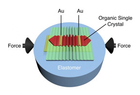 |
| Schematic of wrinkled rubrene single-crystal field-effect transistor. Wrinkles are obtained when in-plane compressive strain is applied on the elastomeric substrate. Electric current between gold (Au) electrodes is modulated by the deformation imposed by the wrinkles. CREDIT: UMass Amherst |
Abstract:
A revolution is coming in flexible electronic technologies as cheaper, more flexible, organic transistors come on the scene to replace expensive, rigid, silicone-based semiconductors, but not enough is known about how bending in these new thin-film electronic devices will affect their performance, say materials scientists at the University of Massachusetts Amherst.
Improving organic transistors that drive flexible and conformable electronics: UMass Amherst scientists advance understanding of strain effects on performance
Amherst. MA | Posted on May 5th, 2015Writing in the current issue of Nature Communications, polymer scientists Alejandro Brise�o and Alfred Crosby at UMass Amherst, with their doctoral student Marcos Reyes-Martinez, now a postdoctoral researcher at Princeton, report results of their recent investigation of how micro-scale wrinkling affects electrical performance in carbon-based, single-crystal semiconductors.
They are the first to apply inhomogeneous deformations, that is strain, to the conducting channel of an organic transistor and to understand the observed effects, says Reyes-Martinez, who conducted the series of experiments as part of his doctoral work.
As he explains, "This is relevant to today's tech industry because transistors drive the logic of all the consumer electronics we use. In the screen on your smart phone, for example, every little pixel that makes up the image is turned on and off by hundreds of thousands or even millions of miniaturized transistors."
"Traditionally, the transistors are rigid, made of an inorganic material such as silicon," he adds. "We're working with a crystalline semiconductor called rubrene, which is an organic, carbon-based material that has performance factors, such as charge-carrier mobility, surpassing those measured in amorphous silicon. Organic semiconductors are an interesting alternative to silicon because their properties can be tuned to make them easily processed, allowing them to coat a variety of surfaces, including soft substrates at relatively low temperatures. As a result, devices based on organic semiconductors are projected to be cheaper since they do not require high temperatures, clean rooms and expensive processing steps like silicon does."
Until now, Reyes-Martinez notes, most researchers have focused on controlling the detrimental effects of mechanical deformation to a transistor's electrical properties. But in their series of systematic experiments, the UMass Amherst team discovered that mechanical deformations only decrease performance under certain conditions, and actually can enhance or have no effect in other instances.
"Our goal was not only to show these effects, but to explain and understand them. What we've done is take advantage of the ordered structure of ultra-thin organic single crystals of rubrene to fabricate high-perfomance, thin-film transistors," he says. "This is the first time that anyone has carried out detailed fundamental work at these length scales with a single crystal."
Though single crystals were once thought to be too fragile for flexible applications, the UMass Amherst team found that crystals ranging in thickness from about 150 nanometers to 1 micrometer were thin enough to be wrinkled and applied to any elastomer substrate. Reyes-Martinez also notes, "Our experiments are especially important because they help scientists working on flexible electronic devices to determine performance limitations of new materials under extreme mechanical deformations, such as when electronic devices conform to skin."
They developed an analytical model based on plate bending theory to quantify the different local strains imposed on the transistor structure by the wrinkle deformations. Using their model they are able to predict how different deformations modulate charge mobility, which no one had quantified before, Reyes-Martinez notes.
These contributions "represent a significant step forward in structure-function relationships in organic semiconductors, critical for the development of the next generation of flexible electronic devices," the authors point out.
####
For more information, please click here
Contacts:
Janet Lathrop
413-545-0444
Copyright © University of Massachusetts at Amherst
If you have a comment, please Contact us.Issuers of news releases, not 7th Wave, Inc. or Nanotechnology Now, are solely responsible for the accuracy of the content.
Bookmark:


| Related News Press |
News and information
![]() Quantum computer improves AI predictions April 17th, 2026
Quantum computer improves AI predictions April 17th, 2026
![]() Flexible sensor gains sensitivity under pressure April 17th, 2026
Flexible sensor gains sensitivity under pressure April 17th, 2026
![]() A reusable chip for particulate matter sensing April 17th, 2026
A reusable chip for particulate matter sensing April 17th, 2026
![]() Detecting vibrational quantum beating in the predissociation dynamics of SF6 using time-resolved photoelectron spectroscopy April 17th, 2026
Detecting vibrational quantum beating in the predissociation dynamics of SF6 using time-resolved photoelectron spectroscopy April 17th, 2026
Flexible Electronics
![]() Flexible sensor gains sensitivity under pressure April 17th, 2026
Flexible sensor gains sensitivity under pressure April 17th, 2026
![]() MXene nanomaterials enter a new dimension Multilayer nanomaterial: MXene flakes created at Drexel University show new promise as 1D scrolls January 30th, 2026
MXene nanomaterials enter a new dimension Multilayer nanomaterial: MXene flakes created at Drexel University show new promise as 1D scrolls January 30th, 2026
![]() Flexible electronics integrated with paper-thin structure for use in space January 17th, 2025
Flexible electronics integrated with paper-thin structure for use in space January 17th, 2025
Thin films
![]() Tiny nanosheets, big leap: A new sensor detects ethanol at ultra-low levels January 30th, 2026
Tiny nanosheets, big leap: A new sensor detects ethanol at ultra-low levels January 30th, 2026
![]() Understanding the mechanism of non-uniform formation of diamond film on tools: Paving the way to a dry process with less environmental impact March 24th, 2023
Understanding the mechanism of non-uniform formation of diamond film on tools: Paving the way to a dry process with less environmental impact March 24th, 2023
![]() New study introduces the best graphite films: The work by Distinguished Professor Feng Ding at UNIST has been published in the October 2022 issue of Nature Nanotechnology November 4th, 2022
New study introduces the best graphite films: The work by Distinguished Professor Feng Ding at UNIST has been published in the October 2022 issue of Nature Nanotechnology November 4th, 2022
![]() Thin-film, high-frequency antenna array offers new flexibility for wireless communications November 5th, 2021
Thin-film, high-frequency antenna array offers new flexibility for wireless communications November 5th, 2021
Hardware
![]() The present and future of computing get a boost from new research July 21st, 2023
The present and future of computing get a boost from new research July 21st, 2023
Chip Technology
![]() A reusable chip for particulate matter sensing April 17th, 2026
A reusable chip for particulate matter sensing April 17th, 2026
![]() Metasurfaces smooth light to boost magnetic sensing precision January 30th, 2026
Metasurfaces smooth light to boost magnetic sensing precision January 30th, 2026
Discoveries
![]() Quantum computer improves AI predictions April 17th, 2026
Quantum computer improves AI predictions April 17th, 2026
![]() Flexible sensor gains sensitivity under pressure April 17th, 2026
Flexible sensor gains sensitivity under pressure April 17th, 2026
![]() A reusable chip for particulate matter sensing April 17th, 2026
A reusable chip for particulate matter sensing April 17th, 2026
![]() Detecting vibrational quantum beating in the predissociation dynamics of SF6 using time-resolved photoelectron spectroscopy April 17th, 2026
Detecting vibrational quantum beating in the predissociation dynamics of SF6 using time-resolved photoelectron spectroscopy April 17th, 2026
Announcements
![]() A fundamentally new therapeutic approach to cystic fibrosis: Nanobody repairs cellular defect April 17th, 2026
A fundamentally new therapeutic approach to cystic fibrosis: Nanobody repairs cellular defect April 17th, 2026
![]() UC Irvine physicists discover method to reverse �quantum scrambling� : The work addresses the problem of information loss in quantum computing system April 17th, 2026
UC Irvine physicists discover method to reverse �quantum scrambling� : The work addresses the problem of information loss in quantum computing system April 17th, 2026
Interviews/Book Reviews/Essays/Reports/Podcasts/Journals/White papers/Posters
![]() A fundamentally new therapeutic approach to cystic fibrosis: Nanobody repairs cellular defect April 17th, 2026
A fundamentally new therapeutic approach to cystic fibrosis: Nanobody repairs cellular defect April 17th, 2026
![]() UC Irvine physicists discover method to reverse �quantum scrambling� : The work addresses the problem of information loss in quantum computing system April 17th, 2026
UC Irvine physicists discover method to reverse �quantum scrambling� : The work addresses the problem of information loss in quantum computing system April 17th, 2026
|
|
||
|
|
||
| The latest news from around the world, FREE | ||
|
|
||
|
|
||
| Premium Products | ||
|
|
||
|
Only the news you want to read!
Learn More |
||
|
|
||
|
Full-service, expert consulting
Learn More |
||
|
|
||