Home > Press > A new spin on spintronics: Michigan team tests radiation-resistant spintronic material, possibly enabling electronic devices that will work in harsh environments
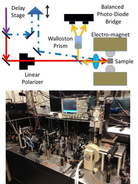 |
| A laser pulse is split into two paths: circularly polarized pump (blue) and linearly polarized probe (red). The pump's path length is adjustable using a delay stage so that the relative arrival time between the pump and probe can be adjusted. After the probe is reflected from the sample surface, the light is passed through a Walloston Prism and sent to a balanced photo-diode bridge. This allows for very sensitive measurements of the Faraday rotation due to electron spin polarizations. CREDIT:AIP Publishing |
Abstract:
A team of researchers from the University of Michigan and Western Michigan University is exploring new materials that could yield higher computational speeds and lower power consumption, even in harsh environments.
A new spin on spintronics: Michigan team tests radiation-resistant spintronic material, possibly enabling electronic devices that will work in harsh environments
Washington, DC | Posted on February 17th, 2015Most modern electronic circuitry relies on controlling electronic charge within a circuit, but this control can easily be disrupted in the presence of radiation, interrupting information processing. Electronics that use spin-based logic, or spintronics, may offer an alternative that is robust even in radiation-filled environments.
Making a radiation-resistant spintronic device requires a material relevant for spintronic applications that can maintain its spin-dependence after it has been irradiated. In a paper published in the journal Applied Physics Letters, from AIP Publishing, the Michigan research team presents their results using bulk Si-doped n-GaAs exposed to proton radiation.
How Does Spintronics Work?
Modern electronic devices use charges to transmit and store information, primarily based upon how many electrons are in one place or another. When a lot of them are at a given terminal, you can call that 'on.' If you have very few of them at the same terminal, you can call that 'off,' just like a light switch. This allows for binary logic depending on whether the terminal is 'on' or 'off.' Spintronics, at its simplest, uses the 'on/off' idea, but instead of counting the electrons, their spin is measured.
"You can think of the spin of an electron as a tiny bar magnet with an arrow painted on it. If the arrow points up, we call that 'spin-up.' If it points down, we call that 'spin-down.' By using light, electric, or magnetic fields, we can manipulate, and measure, the spin direction," said researcher Brennan Pursley, who is the first author of the new study.
While spintronics holds promise for faster and more efficient computation, researchers also want to know whether it would be useful in harsh environments. Currently, radioactivity is a major problem for electronic circuitry because it can scramble information and in the long term degrade electronic properties. For the short term effects, spintronics should be superior: radioactivity can change the quantity of charge in a circuit, but should not affect spin-polarized carriers.
Studying spintronic materials required that the research team combine two well established fields: the study of spin dynamics and the study of radiation damage. Both tool sets are quite robust and have been around for decades but combining the two required sifting through the wealth of radiation damage research. "That was the most difficult aspect," explains Pursley. "It was an entirely new field for us with a variety of established techniques and terminology to learn. The key was to tackle it like any new project: ask a lot of questions, find a few good books or papers, and follow the citations."
Technically, what the Michigan team did was to measure the spin properties of n-GaAs as a function of radiation fluence using time-resolved Kerr rotation and photoluminescence spectroscopy. Results show that the spin lifetime and g-factor of bulk n-GaAs is largely unaffected by proton irradiation making it a candidate for further study for radiation-resistant spintronic devices. The team plans to study other spintronic materials and prototype devices after irradiation since the hybrid field of irradiated spintronics is wide open with plenty of questions to tackle.
Long term, knowledge of radiation effects on spintronic devices will aid in their engineering. A practical implementation would be processing on a communications satellite where without the protection of Earth's atmosphere, electronics can be damaged by harsh solar radiation. The theoretically achievable computation speeds and low power consumption could be combined with compact designs and relatively light shielding. This could make communications systems faster, longer-lived and cheaper to implement.
####
About American Institute of Physics
Applied Physics Letters features concise, rapid reports on significant new findings in applied physics. The journal covers new experimental and theoretical research on applications of physics phenomena related to all branches of science, engineering, and modern technology. See: apl.aip.org
For more information, please click here
Contacts:
Jason Socrates Bardi
240-535-4954
Copyright © American Institute of Physics
If you have a comment, please Contact us.Issuers of news releases, not 7th Wave, Inc. or Nanotechnology Now, are solely responsible for the accuracy of the content.
Bookmark:


| Related Links |
| Related News Press |
News and information
![]() Quantum computer improves AI predictions April 17th, 2026
Quantum computer improves AI predictions April 17th, 2026
![]() Flexible sensor gains sensitivity under pressure April 17th, 2026
Flexible sensor gains sensitivity under pressure April 17th, 2026
![]() A reusable chip for particulate matter sensing April 17th, 2026
A reusable chip for particulate matter sensing April 17th, 2026
![]() Detecting vibrational quantum beating in the predissociation dynamics of SF6 using time-resolved photoelectron spectroscopy April 17th, 2026
Detecting vibrational quantum beating in the predissociation dynamics of SF6 using time-resolved photoelectron spectroscopy April 17th, 2026
Wireless/telecommunications/RF/Antennas/Microwaves
![]() Researchers develop molecular qubits that communicate at telecom frequencies October 3rd, 2025
Researchers develop molecular qubits that communicate at telecom frequencies October 3rd, 2025
![]() HKUST researchers develop new integration technique for efficient coupling of III-V and silicon February 16th, 2024
HKUST researchers develop new integration technique for efficient coupling of III-V and silicon February 16th, 2024
Spintronics
![]() Quantum materials: Electron spin measured for the first time June 9th, 2023
Quantum materials: Electron spin measured for the first time June 9th, 2023
Chip Technology
![]() A reusable chip for particulate matter sensing April 17th, 2026
A reusable chip for particulate matter sensing April 17th, 2026
![]() Metasurfaces smooth light to boost magnetic sensing precision January 30th, 2026
Metasurfaces smooth light to boost magnetic sensing precision January 30th, 2026
Discoveries
![]() Quantum computer improves AI predictions April 17th, 2026
Quantum computer improves AI predictions April 17th, 2026
![]() Flexible sensor gains sensitivity under pressure April 17th, 2026
Flexible sensor gains sensitivity under pressure April 17th, 2026
![]() A reusable chip for particulate matter sensing April 17th, 2026
A reusable chip for particulate matter sensing April 17th, 2026
![]() Detecting vibrational quantum beating in the predissociation dynamics of SF6 using time-resolved photoelectron spectroscopy April 17th, 2026
Detecting vibrational quantum beating in the predissociation dynamics of SF6 using time-resolved photoelectron spectroscopy April 17th, 2026
Announcements
![]() A fundamentally new therapeutic approach to cystic fibrosis: Nanobody repairs cellular defect April 17th, 2026
A fundamentally new therapeutic approach to cystic fibrosis: Nanobody repairs cellular defect April 17th, 2026
![]() UC Irvine physicists discover method to reverse �quantum scrambling� : The work addresses the problem of information loss in quantum computing system April 17th, 2026
UC Irvine physicists discover method to reverse �quantum scrambling� : The work addresses the problem of information loss in quantum computing system April 17th, 2026
Interviews/Book Reviews/Essays/Reports/Podcasts/Journals/White papers/Posters
![]() A fundamentally new therapeutic approach to cystic fibrosis: Nanobody repairs cellular defect April 17th, 2026
A fundamentally new therapeutic approach to cystic fibrosis: Nanobody repairs cellular defect April 17th, 2026
![]() UC Irvine physicists discover method to reverse �quantum scrambling� : The work addresses the problem of information loss in quantum computing system April 17th, 2026
UC Irvine physicists discover method to reverse �quantum scrambling� : The work addresses the problem of information loss in quantum computing system April 17th, 2026
Aerospace/Space
![]() Decoding hydrogen‑bond network of electrolyte for cryogenic durable aqueous zinc‑ion batteries January 30th, 2026
Decoding hydrogen‑bond network of electrolyte for cryogenic durable aqueous zinc‑ion batteries January 30th, 2026
![]() ICFO researchers overcome long-standing bottleneck in single photon detection with twisted 2D materials August 8th, 2025
ICFO researchers overcome long-standing bottleneck in single photon detection with twisted 2D materials August 8th, 2025
![]() Onion-like nanoparticles found in aircraft exhaust May 14th, 2025
Onion-like nanoparticles found in aircraft exhaust May 14th, 2025
Research partnerships
![]() Lab to industry: InSe wafer-scale breakthrough for future electronics August 8th, 2025
Lab to industry: InSe wafer-scale breakthrough for future electronics August 8th, 2025
![]() HKU physicists uncover hidden order in the quantum world through deconfined quantum critical points April 25th, 2025
HKU physicists uncover hidden order in the quantum world through deconfined quantum critical points April 25th, 2025
|
|
||
|
|
||
| The latest news from around the world, FREE | ||
|
|
||
|
|
||
| Premium Products | ||
|
|
||
|
Only the news you want to read!
Learn More |
||
|
|
||
|
Full-service, expert consulting
Learn More |
||
|
|
||