Home > Press > Doped diamond structures offer promise for biotech applications
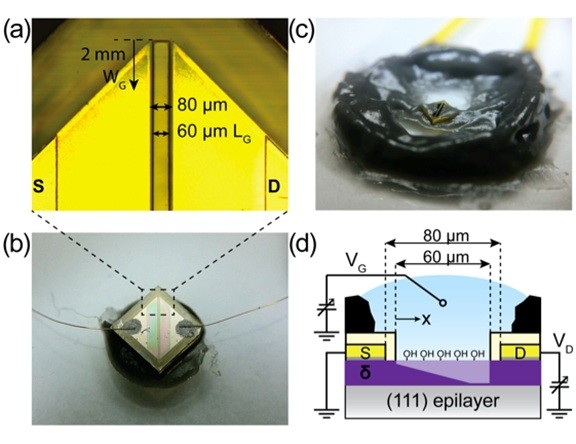 |
| Figure. (a) Micrograph of SGFET source, gate and drain showing passivation openings. (b) Macro photograph of wire bonded device prior to encapsulation. Sample is 2x2 mm. (c) Epoxy encapsulated SGFET. (d) Experimental setup of SGFET using a MESFET analogy, depicting the channel depleted in the saturation regime. |
Abstract:
In a collaboration with Waseda University in Tokyo, LCN researchers have grown highly boron doped diamond layers only 1nm in thickness, a technique known as d-doping, for the realisation of high performance field effect transistors (FETs). When used in a novel configuration, where the normal metal gate that controls the transistor is replaced by an ion containing solution, such devices offer the prospect of highly sensitive detection of biochemical agents, or even action potentials from living cells.
Doped diamond structures offer promise for biotech applications
London, UK | Posted on April 28th, 2012Professor Richard Jackman, who heads the LCNs Diamond Electronics Group, stated "this is the first time that the (111) crystal plane of diamond has been used to generate such heavily doped yet so incredibly thin layers. The resulting transistors offer very good gain and transconductance values when compared to similar devices". The work was performed in a collaboration between the LCN and Professor Kawarada's Diamond Devices team in Japan, with the secondment of Robert Edgington, a PhD student with the LCN team, to Waseda University for five months being made possible through a "Japan Society for the Promotion of Science (JSPS)" award. Robert found the experience valuable beyond just science, "to spend five months immersed in Japanese culture was transforming for me" said Robert, who had the opportunity to practice the Japanese language he had been studying in London prior to his visit. "Diamond surfaces offer a unique platform for chemical functionalisation for the purposes of biosensing" states Professor Jackman, who continued "we have encouraging initial data on the detection of PDGF, a growth factor linked with the promotion of cancer, using aptamers bound to the surface of the gate of the diamond transistor". Robert, who will continue similar work as a Postdoctoral Research Fellow with the UCL Diamond team, added "the work was very hands-on, with the development of diamond growth and doping techniques, the design of FET device structures, and the manipulation of biochemical species, representing a truly interdisciplinary activity".
Boron δ-doped (111) diamond Solution Gate Field Effect Transistors Robert Edgingtona, A. Rahim Ruslindab, Syunsuke Satob, Yuichiro Ishiyamab, Kyosuke Tsugeb, Tasuku Onob, Hiroshi Kawaradab and Richard B. Jackmana*
a London Centre for Nanotechnology, and Department of Electronic and Electrical Engineering, University College London, 17-19 Gordon Street, London, WC1H 0AH, UK
b Department of Electronic and Photonic Systems, Waseda University, Okubo 3-4-1, Shinjuku, Tokyo 169-8555, Japan
* Corresponding author. Tel.: +442076791381; fax: +442076790595 E-mail address: (R. B. Jackman)
####
For more information, please click here
Copyright © London Centre for Nanotechnology
If you have a comment, please Contact us.Issuers of news releases, not 7th Wave, Inc. or Nanotechnology Now, are solely responsible for the accuracy of the content.
Bookmark:


| Related Links |
| Related News Press |
News and information
![]() Quantum computer improves AI predictions April 17th, 2026
Quantum computer improves AI predictions April 17th, 2026
![]() Flexible sensor gains sensitivity under pressure April 17th, 2026
Flexible sensor gains sensitivity under pressure April 17th, 2026
![]() A reusable chip for particulate matter sensing April 17th, 2026
A reusable chip for particulate matter sensing April 17th, 2026
![]() Detecting vibrational quantum beating in the predissociation dynamics of SF6 using time-resolved photoelectron spectroscopy April 17th, 2026
Detecting vibrational quantum beating in the predissociation dynamics of SF6 using time-resolved photoelectron spectroscopy April 17th, 2026
Chip Technology
![]() A reusable chip for particulate matter sensing April 17th, 2026
A reusable chip for particulate matter sensing April 17th, 2026
![]() Metasurfaces smooth light to boost magnetic sensing precision January 30th, 2026
Metasurfaces smooth light to boost magnetic sensing precision January 30th, 2026
Nanomedicine
![]() A fundamentally new therapeutic approach to cystic fibrosis: Nanobody repairs cellular defect April 17th, 2026
A fundamentally new therapeutic approach to cystic fibrosis: Nanobody repairs cellular defect April 17th, 2026
![]() New molecular technology targets tumors and simultaneously silences two �undruggable� cancer genes August 8th, 2025
New molecular technology targets tumors and simultaneously silences two �undruggable� cancer genes August 8th, 2025
![]() New imaging approach transforms study of bacterial biofilms August 8th, 2025
New imaging approach transforms study of bacterial biofilms August 8th, 2025
![]() Electrifying results shed light on graphene foam as a potential material for lab grown cartilage June 6th, 2025
Electrifying results shed light on graphene foam as a potential material for lab grown cartilage June 6th, 2025
Sensors
![]() Flexible sensor gains sensitivity under pressure April 17th, 2026
Flexible sensor gains sensitivity under pressure April 17th, 2026
![]() Tiny nanosheets, big leap: A new sensor detects ethanol at ultra-low levels January 30th, 2026
Tiny nanosheets, big leap: A new sensor detects ethanol at ultra-low levels January 30th, 2026
![]() From sensors to smart systems: the rise of AI-driven photonic noses January 30th, 2026
From sensors to smart systems: the rise of AI-driven photonic noses January 30th, 2026
![]() Sensors innovations for smart lithium-based batteries: advancements, opportunities, and potential challenges August 8th, 2025
Sensors innovations for smart lithium-based batteries: advancements, opportunities, and potential challenges August 8th, 2025
Discoveries
![]() Quantum computer improves AI predictions April 17th, 2026
Quantum computer improves AI predictions April 17th, 2026
![]() Flexible sensor gains sensitivity under pressure April 17th, 2026
Flexible sensor gains sensitivity under pressure April 17th, 2026
![]() A reusable chip for particulate matter sensing April 17th, 2026
A reusable chip for particulate matter sensing April 17th, 2026
![]() Detecting vibrational quantum beating in the predissociation dynamics of SF6 using time-resolved photoelectron spectroscopy April 17th, 2026
Detecting vibrational quantum beating in the predissociation dynamics of SF6 using time-resolved photoelectron spectroscopy April 17th, 2026
Announcements
![]() A fundamentally new therapeutic approach to cystic fibrosis: Nanobody repairs cellular defect April 17th, 2026
A fundamentally new therapeutic approach to cystic fibrosis: Nanobody repairs cellular defect April 17th, 2026
![]() UC Irvine physicists discover method to reverse �quantum scrambling� : The work addresses the problem of information loss in quantum computing system April 17th, 2026
UC Irvine physicists discover method to reverse �quantum scrambling� : The work addresses the problem of information loss in quantum computing system April 17th, 2026
Alliances/Trade associations/Partnerships/Distributorships
![]() Chicago Quantum Exchange welcomes six new partners highlighting quantum technology solutions, from Chicago and beyond September 23rd, 2022
Chicago Quantum Exchange welcomes six new partners highlighting quantum technology solutions, from Chicago and beyond September 23rd, 2022
![]() University of Illinois Chicago joins Brookhaven Lab's Quantum Center June 10th, 2022
University of Illinois Chicago joins Brookhaven Lab's Quantum Center June 10th, 2022
Research partnerships
![]() Lab to industry: InSe wafer-scale breakthrough for future electronics August 8th, 2025
Lab to industry: InSe wafer-scale breakthrough for future electronics August 8th, 2025
![]() HKU physicists uncover hidden order in the quantum world through deconfined quantum critical points April 25th, 2025
HKU physicists uncover hidden order in the quantum world through deconfined quantum critical points April 25th, 2025
|
|
||
|
|
||
| The latest news from around the world, FREE | ||
|
|
||
|
|
||
| Premium Products | ||
|
|
||
|
Only the news you want to read!
Learn More |
||
|
|
||
|
Full-service, expert consulting
Learn More |
||
|
|
||