Home > Press > Semiconductor manufacturing technique holds promise for solar energy
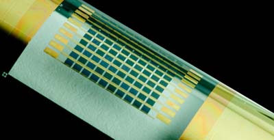 |
| A flexible array of gallium arsenide solar cells. Gallium arsenide and other compound semiconductors are more efficient than the more commonly used silicon. Photo courtesy John Rogers |
Abstract:
Thanks to a new semiconductor manufacturing method pioneered at the University of Illinois, the future of solar energy just got brighter
Semiconductor manufacturing technique holds promise for solar energy
Champaign, IL | Posted on May 20th, 2010Although silicon is the industry standard semiconductor in most electronic devices, including the photovoltaic cells that solar panels use to convert sunlight into energy, it is hardly the most efficient material available. For example, the semiconductor gallium arsenide and related compound semiconductors offer nearly twice the efficiency as silicon in solar devices, yet they are rarely used in utility-scale applications because of their high manufacturing cost.
U. of I. professors John Rogers and Xiuling Li explored lower-cost ways to manufacture thin films of gallium arsenide that also allowed versatility in the types of devices they could be incorporated into. "If you can reduce substantially the cost of gallium arsenide and other compound semiconductors, then you could expand their range of applications," said Rogers, the Lee J. Flory Founder Chair in Engineering Innovation, and a professor of materials science and engineering and of chemistry.
Typically, gallium arsenide is deposited in a single thin layer on a small wafer. Either the desired device is made directly on the wafer, or the semiconductor-coated wafer is cut up into chips of the desired size. The Illinois group decided to deposit multiple layers of the material on a single wafer, creating a layered, "pancake" stack of gallium arsenide thin films.
"If you grow 10 layers in one growth, you only have to load the wafer one time," said Li, a professor of electrical and computer engineering. "If you do this in 10 growths, loading and unloading with temperature ramp-up and ramp-down take a lot of time. If you consider what is required for each growth - the machine, the preparation, the time, the people - the overhead saving our approach offers is a significant cost reduction."
Next the researchers individually peel off the layers and transfer them. To accomplish this, the stacks alternate layers of aluminum arsenide with the gallium arsenide. Bathing the stacks in a solution of acid and an oxidizing agent dissolves the layers of aluminum arsenide, freeing the individual thin sheets of gallium arsenide. A soft stamp-like device picks up the layers, one at a time from the top down, for transfer to another substrate - glass, plastic or silicon, depending on the application. Then the wafer can be reused for another growth.
"By doing this we can generate much more material more rapidly and more cost effectively," Rogers said. "We're creating bulk quantities of material, as opposed to just the thin single-layer manner in which it is typically grown."
Freeing the material from the wafer also opens the possibility of flexible, thin-film electronics made with gallium arsenide or other high-speed semiconductors. "To make devices that can conform but still retain high performance, that's significant," Li said.
In a paper to be published online May 20 in the journal Nature, the group describes its methods and demonstrates three types of devices using gallium arsenide chips manufactured in multilayer stacks: light sensors, high-speed transistors and solar cells. The authors also provide a detailed cost comparison.
Another advantage of the multilayer technique is the release from area constraints, especially important for solar cells. As the layers are removed from the stack, they can be laid out side-by-side on another substrate to produce a much larger surface area, whereas the typical single-layer process limits area to the size of the wafer.
"For photovoltaics, you want large area coverage to catch as much sunlight as possible. In an extreme case we might grow enough layers to have 10 times the area of the conventional route," Rogers said.
"You really multiply the area coverage, and by a similar multiplier you reduce the cost, while at the same time eliminating the consumption of the wafer," he said.
Among the paper's co-authors are two scientists from Semprius Inc., a North Carolina-based startup company that is beginning to use this technique to manufacture solar cells. A shift from silicon-based panels to more efficient gallium arsenide models could make solar power a more cost-effective form of alternative energy.
Next, the group plans to explore more potential device applications and other semiconductor materials that could adapt to multilayer growth.
The Department of Energy and National Science Foundation-funded team also includes U. of I. postdoctoral researchers Jongseung Yoon, Sungjin Jo and Inhwa Jung; students Ik Su Chun and Hoon-Sik Kin; and electrical and computer engineering professor James Coleman, along with Ungyu Paik, of Hanyang University in Seoul, and Semprius scientists Matthew Meitl and Etienne Menard.
####
For more information, please click here
Contacts:
Liz Ahlberg
Physical Sciences Editor
217-244-1073
Copyright © University of Illinois
If you have a comment, please Contact us.Issuers of news releases, not 7th Wave, Inc. or Nanotechnology Now, are solely responsible for the accuracy of the content.
Bookmark:


| Related News Press |
News and information
![]() Quantum computer improves AI predictions April 17th, 2026
Quantum computer improves AI predictions April 17th, 2026
![]() Flexible sensor gains sensitivity under pressure April 17th, 2026
Flexible sensor gains sensitivity under pressure April 17th, 2026
![]() A reusable chip for particulate matter sensing April 17th, 2026
A reusable chip for particulate matter sensing April 17th, 2026
![]() Detecting vibrational quantum beating in the predissociation dynamics of SF6 using time-resolved photoelectron spectroscopy April 17th, 2026
Detecting vibrational quantum beating in the predissociation dynamics of SF6 using time-resolved photoelectron spectroscopy April 17th, 2026
Thin films
![]() Tiny nanosheets, big leap: A new sensor detects ethanol at ultra-low levels January 30th, 2026
Tiny nanosheets, big leap: A new sensor detects ethanol at ultra-low levels January 30th, 2026
![]() Utilizing palladium for addressing contact issues of buried oxide thin film transistors April 5th, 2024
Utilizing palladium for addressing contact issues of buried oxide thin film transistors April 5th, 2024
![]() Understanding the mechanism of non-uniform formation of diamond film on tools: Paving the way to a dry process with less environmental impact March 24th, 2023
Understanding the mechanism of non-uniform formation of diamond film on tools: Paving the way to a dry process with less environmental impact March 24th, 2023
![]() New study introduces the best graphite films: The work by Distinguished Professor Feng Ding at UNIST has been published in the October 2022 issue of Nature Nanotechnology November 4th, 2022
New study introduces the best graphite films: The work by Distinguished Professor Feng Ding at UNIST has been published in the October 2022 issue of Nature Nanotechnology November 4th, 2022
Possible Futures
![]() A fundamentally new therapeutic approach to cystic fibrosis: Nanobody repairs cellular defect April 17th, 2026
A fundamentally new therapeutic approach to cystic fibrosis: Nanobody repairs cellular defect April 17th, 2026
![]() UC Irvine physicists discover method to reverse �quantum scrambling� : The work addresses the problem of information loss in quantum computing system April 17th, 2026
UC Irvine physicists discover method to reverse �quantum scrambling� : The work addresses the problem of information loss in quantum computing system April 17th, 2026
Academic/Education
![]() Rice University launches Rice Synthetic Biology Institute to improve lives January 12th, 2024
Rice University launches Rice Synthetic Biology Institute to improve lives January 12th, 2024
![]() Multi-institution, $4.6 million NSF grant to fund nanotechnology training September 9th, 2022
Multi-institution, $4.6 million NSF grant to fund nanotechnology training September 9th, 2022
Chip Technology
![]() A reusable chip for particulate matter sensing April 17th, 2026
A reusable chip for particulate matter sensing April 17th, 2026
![]() Metasurfaces smooth light to boost magnetic sensing precision January 30th, 2026
Metasurfaces smooth light to boost magnetic sensing precision January 30th, 2026
Announcements
![]() A fundamentally new therapeutic approach to cystic fibrosis: Nanobody repairs cellular defect April 17th, 2026
A fundamentally new therapeutic approach to cystic fibrosis: Nanobody repairs cellular defect April 17th, 2026
![]() UC Irvine physicists discover method to reverse �quantum scrambling� : The work addresses the problem of information loss in quantum computing system April 17th, 2026
UC Irvine physicists discover method to reverse �quantum scrambling� : The work addresses the problem of information loss in quantum computing system April 17th, 2026
Energy
![]() Sensors innovations for smart lithium-based batteries: advancements, opportunities, and potential challenges August 8th, 2025
Sensors innovations for smart lithium-based batteries: advancements, opportunities, and potential challenges August 8th, 2025
![]() Simple algorithm paired with standard imaging tool could predict failure in lithium metal batteries August 8th, 2025
Simple algorithm paired with standard imaging tool could predict failure in lithium metal batteries August 8th, 2025
Solar/Photovoltaic
![]() Spinel-type sulfide semiconductors to operate the next-generation LEDs and solar cells For solar-cell absorbers and green-LED source October 3rd, 2025
Spinel-type sulfide semiconductors to operate the next-generation LEDs and solar cells For solar-cell absorbers and green-LED source October 3rd, 2025
![]() KAIST researchers introduce new and improved, next-generation perovskite solar cell November 8th, 2024
KAIST researchers introduce new and improved, next-generation perovskite solar cell November 8th, 2024
![]() Groundbreaking precision in single-molecule optoelectronics August 16th, 2024
Groundbreaking precision in single-molecule optoelectronics August 16th, 2024
![]() Development of zinc oxide nanopagoda array photoelectrode: photoelectrochemical water-splitting hydrogen production January 12th, 2024
Development of zinc oxide nanopagoda array photoelectrode: photoelectrochemical water-splitting hydrogen production January 12th, 2024
|
|
||
|
|
||
| The latest news from around the world, FREE | ||
|
|
||
|
|
||
| Premium Products | ||
|
|
||
|
Only the news you want to read!
Learn More |
||
|
|
||
|
Full-service, expert consulting
Learn More |
||
|
|
||