Home > Press > Graphene Films Clear Major Fabrication Hurdle
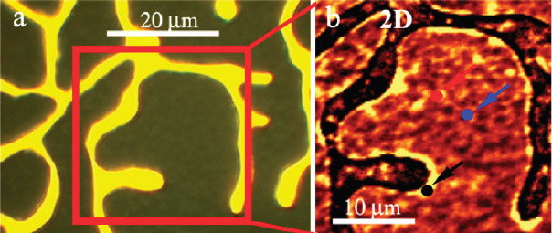 |
| (a) Optical image of a CVD graphene film on a copper layer showing the finger morphology of the metal; (b) Raman 2D band map of the graphene film between the copper fingers over the area marked by the red square on left. (image from Yuegang Zhang) |
Abstract:
Graphene, the two-dimensional crystalline form of carbon, is a potential superstar for the electronics industry. With freakishly mobile electrons that can blaze through the material at nearly the speed of light - 100 times faster than electrons can move through silicon - graphene could be used to make superfast transistors or computer memory chips. Graphene's unique "chicken wire" atomic structure exhibits incredible flexibility and mechanical strength, as well as unusual optical properties that could open a number of promising doors in both the electronics and the photonics industries. However, among the hurdles preventing graphite from joining the pantheon of star high-tech materials, perhaps none looms larger than just learning to make the stuff in high quality and usable quantities.
Graphene Films Clear Major Fabrication Hurdle
Berkeley, CA | Posted on April 10th, 2010"Before we can fully utilize the superior electronic properties of graphene in devices, we must first develop a method of forming uniform single-layer graphene films on nonconducting substrates on a large scale," says Yuegang Zhang, a materials scientist with the Lawrence Berkeley National Laboratory (Berkeley Lab). Current fabrication methods based on mechanical cleavage or ultrahigh vacuum annealing, he says, are ill-suited for commercial-scale production. Graphene films made via solution-based deposition and chemical reduction have suffered from poor or uneven quality.
Zhang and colleagues at Berkeley Lab's Molecular Foundry, a U.S. Department of Energy (DOE) center for nanoscience, have taken a significant step at clearing this major hurdle. They have successfully used direct chemical vapor deposition (CVD) to synthesize single-layer films of graphene on a dielectric substrate. Zhang and his colleagues made their graphene films by catalytically decomposing hydrocarbon precursors over thin films of copper that had been pre-deposited on the dielectric substrate. The copper films subsequently dewetted (separated into puddles or droplets) and were evaporated. The final product was a single-layer graphene film on a bare dielectric.
"This is exciting news for electronic applications because chemical vapor deposition is a technique already widely used in the semiconductor industry," Zhang says.
"Also, we can learn more about the growth of graphene on metal catalyst surfaces by observing the evolution of the films after the evaporation of the copper. This should lay an important foundation for further control of the process and enable us to tailor the properties of these films or produce desired morphologies, such as graphene nanoribbons."
Zhang and his colleagues have reported their findings in the journal Nano Letters in a paper titled, "Direct Chemical Vapor Deposition of Graphene on Dielectric Surfaces." Other co-authors of this paper were Ariel Ismach, Clara Druzgalski, Samuel Penwell, Maxwell Zheng, Ali Javey and Jeffrey Bokor, all with Berkeley Lab.
In their study, Zhang and his colleagues used electron-beam evaporation to deposit copper films ranging in thickness from 100 to 450 nanometers. Copper was chosen because as a low carbon solubility metal catalyst it was expected to allow better control over the number of graphene layers produced. Several different dielectric substrates were evaluated including single-crystal quartz, sapphire, fused silica and silicon oxide wafers. CVD of the graphene was carried out at 1,000 degrees Celsius in durations that ranged from 15 minutes up to seven hours.
"This was done to allow us to study the effect of film thickness, substrate type and CVD growth time on the graphene formation," Zhang says.
A combination of scanning Raman mapping and spectroscopy, plus scanning electron and atomic force microscopy confirmed the presence of continuous single-layer graphene films coating metal-free areas of dielectric substrate measuring tens of square micrometers.
"Further improvement on the control of the dewetting and evaporation process could lead to the direct deposition of patterned graphene for large-scale electronic device fabrication, Zhang says. "This method could also be generalized and used to deposit other two-dimensional materials, such as boron-nitride."
Even the appearance of wrinkles in the graphene films that followed along the lines of the dewetting shape of the copper could prove to be beneficial in the long-run. Although previous studies have indicated that wrinkles in a graphene film have a negative impact on electronic properties by introducing strains that reduce electron mobility, Zhang believes the wrinkles can be turned to an advantage.
"If we can learn to control the formation of wrinkles in our films, we should be able to modulate the resulting strain and thereby tailor electronic properties," he says.
"Further study of the wrinkle formation could also give us important new clues for the formation of graphene nanoribbons."
This work was primarily supported by the DOE Office of Science.
The Molecular Foundry is one of the five DOE Nanoscale Science Research Centers (NSRCs), premier national user facilities for interdisciplinary research at the nanoscale. Together the NSRCs comprise a suite of complementary facilities that provide researchers with state-of-the-art capabilities to fabricate, process, characterize and model nanoscale materials, and constitute the largest infrastructure investment of the National Nanotechnology Initiative. The NSRCs are located at DOE's Argonne, Brookhaven, Lawrence Berkeley, Oak Ridge and Sandia and Los Alamos National Laboratories.
####
About Berkeley Lab
Berkeley Lab is a U.S. Department of Energy national laboratory located in Berkeley, California. It conducts unclassified scientific research and is managed by the University of California. Visit our website at www.lbl.gov.
For more information, please click here
Contacts:
Lynn Yarris
(510) 486-5375
Copyright © Berkeley Lab
If you have a comment, please Contact us.Issuers of news releases, not 7th Wave, Inc. or Nanotechnology Now, are solely responsible for the accuracy of the content.
Bookmark:


| Related News Press |
News and information
![]() Quantum computer improves AI predictions April 17th, 2026
Quantum computer improves AI predictions April 17th, 2026
![]() Flexible sensor gains sensitivity under pressure April 17th, 2026
Flexible sensor gains sensitivity under pressure April 17th, 2026
![]() A reusable chip for particulate matter sensing April 17th, 2026
A reusable chip for particulate matter sensing April 17th, 2026
![]() Detecting vibrational quantum beating in the predissociation dynamics of SF6 using time-resolved photoelectron spectroscopy April 17th, 2026
Detecting vibrational quantum beating in the predissociation dynamics of SF6 using time-resolved photoelectron spectroscopy April 17th, 2026
Govt.-Legislation/Regulation/Funding/Policy
![]() Quantum computer improves AI predictions April 17th, 2026
Quantum computer improves AI predictions April 17th, 2026
![]() Metasurfaces smooth light to boost magnetic sensing precision January 30th, 2026
Metasurfaces smooth light to boost magnetic sensing precision January 30th, 2026
![]() New imaging approach transforms study of bacterial biofilms August 8th, 2025
New imaging approach transforms study of bacterial biofilms August 8th, 2025
Possible Futures
![]() A fundamentally new therapeutic approach to cystic fibrosis: Nanobody repairs cellular defect April 17th, 2026
A fundamentally new therapeutic approach to cystic fibrosis: Nanobody repairs cellular defect April 17th, 2026
![]() UC Irvine physicists discover method to reverse �quantum scrambling� : The work addresses the problem of information loss in quantum computing system April 17th, 2026
UC Irvine physicists discover method to reverse �quantum scrambling� : The work addresses the problem of information loss in quantum computing system April 17th, 2026
Chip Technology
![]() A reusable chip for particulate matter sensing April 17th, 2026
A reusable chip for particulate matter sensing April 17th, 2026
![]() Metasurfaces smooth light to boost magnetic sensing precision January 30th, 2026
Metasurfaces smooth light to boost magnetic sensing precision January 30th, 2026
Nanotubes/Buckyballs/Fullerenes/Nanorods/Nanostrings/Nanosheets
![]() Tiny nanosheets, big leap: A new sensor detects ethanol at ultra-low levels January 30th, 2026
Tiny nanosheets, big leap: A new sensor detects ethanol at ultra-low levels January 30th, 2026
![]() Enhancing power factor of p- and n-type single-walled carbon nanotubes April 25th, 2025
Enhancing power factor of p- and n-type single-walled carbon nanotubes April 25th, 2025
![]() Chainmail-like material could be the future of armor: First 2D mechanically interlocked polymer exhibits exceptional flexibility and strength January 17th, 2025
Chainmail-like material could be the future of armor: First 2D mechanically interlocked polymer exhibits exceptional flexibility and strength January 17th, 2025
![]() Innovative biomimetic superhydrophobic coating combines repair and buffering properties for superior anti-erosion December 13th, 2024
Innovative biomimetic superhydrophobic coating combines repair and buffering properties for superior anti-erosion December 13th, 2024
Nanoelectronics
![]() Lab to industry: InSe wafer-scale breakthrough for future electronics August 8th, 2025
Lab to industry: InSe wafer-scale breakthrough for future electronics August 8th, 2025
![]() Interdisciplinary: Rice team tackles the future of semiconductors Multiferroics could be the key to ultralow-energy computing October 6th, 2023
Interdisciplinary: Rice team tackles the future of semiconductors Multiferroics could be the key to ultralow-energy computing October 6th, 2023
![]() Key element for a scalable quantum computer: Physicists from Forschungszentrum J�lich and RWTH Aachen University demonstrate electron transport on a quantum chip September 23rd, 2022
Key element for a scalable quantum computer: Physicists from Forschungszentrum J�lich and RWTH Aachen University demonstrate electron transport on a quantum chip September 23rd, 2022
![]() Reduced power consumption in semiconductor devices September 23rd, 2022
Reduced power consumption in semiconductor devices September 23rd, 2022
Announcements
![]() A fundamentally new therapeutic approach to cystic fibrosis: Nanobody repairs cellular defect April 17th, 2026
A fundamentally new therapeutic approach to cystic fibrosis: Nanobody repairs cellular defect April 17th, 2026
![]() UC Irvine physicists discover method to reverse �quantum scrambling� : The work addresses the problem of information loss in quantum computing system April 17th, 2026
UC Irvine physicists discover method to reverse �quantum scrambling� : The work addresses the problem of information loss in quantum computing system April 17th, 2026
|
|
||
|
|
||
| The latest news from around the world, FREE | ||
|
|
||
|
|
||
| Premium Products | ||
|
|
||
|
Only the news you want to read!
Learn More |
||
|
|
||
|
Full-service, expert consulting
Learn More |
||
|
|
||