Home > Press > IBM Brings Nature to Computer Chip Manufacturing
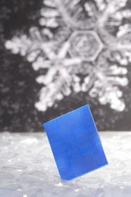 |
| IBM Airgap Microprocessor -- This thumbnail-size IBM chip was created by harnessing the natural forces that make patterns including snowflakes and sea shells. The self-assembly technology is being used to create a vacuum between the miles of on-chip wiring. IBM expects to begin manufacturing more powerful and energy-efficient servers based on airgap-technology microprocessors beginning in 2009. |
Abstract:
First-Ever Manufacturing Application of "Self Assembly" Used to Create a Vacuum -- the Ultimate Insulator -- Around Nanowires for Next-Generation Microprocessors
IBM Brings Nature to Computer Chip Manufacturing
ARMONK, NY | Posted on May 2nd, 2007IBM (NYSE: IBM) today announced the first-ever application of a breakthrough self-assembling nanotechnology to conventional chip manufacturing, borrowing a process from nature to build the next generation computer chips.
The natural pattern-creating process that forms seashells, snowflakes, and enamel on teeth has been harnessed by IBM to form trillions of holes to create insulating vacuums around the miles of nano-scale wires packed next to each other inside each computer chip.
In chips running in IBM labs using the technique, the researchers have proven that the electrical signals on the chips can flow 35 percent faster, or the chips can consume 15 percent less energy compared to the most advanced chips using conventional techniques.
The IBM patented self-assembly process moves a nanotechnology manufacturing method that had shown promise in laboratories into a commercial manufacturing environment for the first time, providing the equivalent of two generations of Moore's Law wiring performance improvements in a single step, using conventional manufacturing techniques.
This new form of insulation, commonly referred to as "airgaps" by scientists, is a misnomer, as the gaps are actually a vacuum, absent of air. The technique deployed by IBM causes a vacuum to form between the copper wires on a computer chip, allowing electrical signals to flow faster, while consuming less electrical power. The self-assembly process enables the nano-scale patterning required to form the gaps; this patterning is considerably smaller than current lithographic techniques can achieve.
A vacuum is believed to be the ultimate insulator for what is known as wiring capacitance, which occurs when two conductors, in this case adjacent wires on a chip, sap or siphon electrical energy from one another, generating undesirable heat and slowing the speed at which data can move through a chip.
Until now, chip designers often were forced to fight capacitance issues by pushing ever more power through chips creating, in the process, a range of other problems. They have also used insulators with better insulating capability, but these insulators have become tenuously fragile as chip features get smaller and smaller, and their insulating properties do not compare to those of a vacuum.
The self-assembly process already has been integrated with IBM's state-of-the-art manufacturing line in East Fishkill, New York and is expected to be fully incorporated in IBM's manufacturing lines and used in chips in 2009. The chips will be used in IBM's server product lines and thereafter for chips IBM builds for other companies.
"This is the first time anyone has proven the ability to synthesize mass quantities of these self-assembled polymers and integrate them into an existing manufacturing process with great yield results," said Dan Edelstein, IBM Fellow and chief scientist of the self-assembly airgap project. "By moving self assembly from the lab to the fab, we are able to make chips that are smaller, faster and consume less power than existing materials and design architectures allow."
Edelstein led the IBM team that invented the technique to use copper wiring in computer chips instead of aluminum, now a standard method for producing chips, ushering in a decade of chip innovations from the IBM labs that transformed how chips were built and used across many industries and applications.
The Secret of Self Assembly
The secret of IBM's breakthrough lies in how the IBM scientists moved the self-assembly process from the laboratory to a production manufacturing environment in a way that can potentially yield millions of chips with consistent, high performance results.
Today, chips are manufactured with copper wiring surrounded by an insulator, which involves using a mask to create circuit patterns by beaming light through the mask and later chemically removing the parts that are not needed.
The new technique to make airgaps by self-assembly skips the masking and light-etching process. Instead IBM scientists discovered the right mix of compounds, which they pour onto a silicon wafer with the wired chip patterns, then bake it.
This patented process provides the right environment for the compounds to assemble in a directed manner, creating trillions of uniform, nano-scale holes across an entire 300-millimeter wafer. These holes are just 20 nanometers in diameter, up to five times smaller than would be possible using today's most advanced lithography technique.
Once the holes are formed, the carbon silicate glass is removed, creating a vacuum between the wires -- known as the airgap -- allowing the electrical signals to either flow 35 percent faster, or to consume 15 percent less energy.
Self assembly is a concept scientists have been studying at IBM and in labs around the world as a potential technique to create materials useful for building computer chips. The concept occurs in nature every day, it is how enamel is formed on our teeth, the process that creates seashells and is what transforms water into complex snowflakes. The major difference is, while the processes that occur in nature are all unique, IBM has been able to direct the self-assembly process to form trillions of holes that are all similar.
This new technology can be incorporated into any standard CMOS manufacturing line, without disruption or new tooling. The self assembly process was jointly invented between IBM's Almaden Research Center in San Jose, California and the T.J. Watson Research Center in Yorktown, New York. The technique was perfected for future commercial production at the College of Nanoscale Science and Engineering of the University at Albany, within the world-class Albany NanoTech facilities, a research and development site in Albany, New York with strong ties to IBM, and at IBM's Semiconductor Research and Development Center in East Fishkill, N.Y.
####
About IBM
Note to Editors: Broadcast-quality video on airgap can be downloaded by journalists at http://www.thenewsmarket.com/ibm. Photos and related materials are available in the IBM Press Room at http://www-03.ibm.com/press/us/en/presskit/21463.wss.
For further information about IBM Microelectronics, visit http://www.ibm.com/chips/
For more information about IBM Research, visit http://www.ibm.com/research
For more information, please click here
Contacts:
Bruce McConnel
IBM Media Relations
914-766-4427 (o)
203-739-5462 (m)
Copyright © Market Wire
If you have a comment, please Contact us.Issuers of news releases, not 7th Wave, Inc. or Nanotechnology Now, are solely responsible for the accuracy of the content.
Bookmark:


| Related News Press |
Chip Technology
![]() A reusable chip for particulate matter sensing April 17th, 2026
A reusable chip for particulate matter sensing April 17th, 2026
![]() Metasurfaces smooth light to boost magnetic sensing precision January 30th, 2026
Metasurfaces smooth light to boost magnetic sensing precision January 30th, 2026
Self Assembly
![]() Diamond glitter: A play of colors with artificial DNA crystals May 17th, 2024
Diamond glitter: A play of colors with artificial DNA crystals May 17th, 2024
![]() Liquid crystal templated chiral nanomaterials October 14th, 2022
Liquid crystal templated chiral nanomaterials October 14th, 2022
![]() Nanoclusters self-organize into centimeter-scale hierarchical assemblies April 22nd, 2022
Nanoclusters self-organize into centimeter-scale hierarchical assemblies April 22nd, 2022
![]() Atom by atom: building precise smaller nanoparticles with templates March 4th, 2022
Atom by atom: building precise smaller nanoparticles with templates March 4th, 2022
Nanoelectronics
![]() Lab to industry: InSe wafer-scale breakthrough for future electronics August 8th, 2025
Lab to industry: InSe wafer-scale breakthrough for future electronics August 8th, 2025
![]() Interdisciplinary: Rice team tackles the future of semiconductors Multiferroics could be the key to ultralow-energy computing October 6th, 2023
Interdisciplinary: Rice team tackles the future of semiconductors Multiferroics could be the key to ultralow-energy computing October 6th, 2023
![]() Key element for a scalable quantum computer: Physicists from Forschungszentrum J�lich and RWTH Aachen University demonstrate electron transport on a quantum chip September 23rd, 2022
Key element for a scalable quantum computer: Physicists from Forschungszentrum J�lich and RWTH Aachen University demonstrate electron transport on a quantum chip September 23rd, 2022
![]() Reduced power consumption in semiconductor devices September 23rd, 2022
Reduced power consumption in semiconductor devices September 23rd, 2022
Announcements
![]() A fundamentally new therapeutic approach to cystic fibrosis: Nanobody repairs cellular defect April 17th, 2026
A fundamentally new therapeutic approach to cystic fibrosis: Nanobody repairs cellular defect April 17th, 2026
![]() UC Irvine physicists discover method to reverse �quantum scrambling� : The work addresses the problem of information loss in quantum computing system April 17th, 2026
UC Irvine physicists discover method to reverse �quantum scrambling� : The work addresses the problem of information loss in quantum computing system April 17th, 2026
|
|
||
|
|
||
| The latest news from around the world, FREE | ||
|
|
||
|
|
||
| Premium Products | ||
|
|
||
|
Only the news you want to read!
Learn More |
||
|
|
||
|
Full-service, expert consulting
Learn More |
||
|
|
||