Home > Press > Shrinking hydrogels enlarge nanofabrication options: Researchers from Pittsburgh and Hong Kong print intricate, 2D and 3D patterns
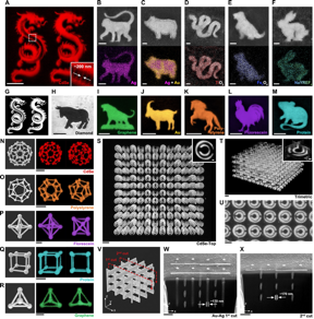 |
| (A) Fluorescent image of two dragons of CdSe QDs without shrinking; the inset shows a resolution of ~200 nm. (B-F) SEM (top) and EDX (bottom) images of a monkey of Ag; pig of Au-Ag alloy; snake of TiO2; dog of Fe3O4; and rabbit of NaYREF4, respectively. (G) Designed dragon patterns in (A). (H) Optical microscopy image of an ox of diamond. (I-M) Fluorescent images of a tiger of graphene QDs; goat of fluorescent Au; horse of polystyrene; rooster of fluorescein; and mouse of fluorescent protein, respectively. (N-R) 3D models and fluorescent images (maximum-intensity projection) of the fabricated structures in shapes of a C60 molecule, regular dodecahedron, regular octahedron, cube, and regular tetrahedron of different materials, respectively. (S) Top view of a five-layer split ring resonator (SRR) structure; inset: SRR unit; and (T) trimetric view of the SRR structure; inset: slice view of an SRR unit. (U) SEM image of the top layer of an SRR structure after shrinking and dehydration. (V) 3D model of a woodpile structure containing 16 vertical rods along the z-axis. (W, X) SEM cross-sectional images of the fabricated woodpile at the two cut planes in (V), respectively. (Substrate tilt angle: 52°). Scale bars are 1 µm for (B-F, U, W, X, and the insets of S and T); and 10 µm for (A, H-M, N-T). CREDIT Chinese University of Hong Kong |
Abstract:
Carnegie Mellon University’s Yongxin (Leon) Zhao and the Chinese University of Hong Kong’s Shih-Chi Chen have a big idea for manufacturing nanodevices.
Shrinking hydrogels enlarge nanofabrication options: Researchers from Pittsburgh and Hong Kong print intricate, 2D and 3D patterns
Pittsburgh, PA and Hong Kong, China | Posted on December 29th, 2022Zhao’s Biophotonics Lab develops novel techniques to study biological and pathological processes in cells and tissues. Through a process called expansion microscopy, the lab works to advance techniques to proportionally enlarge microscopic samples embedded in a hydrogel, allowing researchers to be able to view fine details without upgrading their microscopes.
In 2019, an inspiring conversation with Shih-Chi Chen, who was visiting Carnegie Mellon as an invited speaker and is a professor at the Chinese University of Hong Kong’s Department of Mechanical and Automation Engineering, sparked a collaboration between the two researchers. They thought they could use their combined expertise to find novel solutions for the long-standing challenge in microfabrication: developing ways to reduce the size of printable nanodevices to as small as 10s of nanometers or several atoms thick.
Their solution is the opposite of expansion microscopy: create the 3D pattern of a material in hydrogel and shrink it for nanoscale resolution.
“Shih-Chi is known for inventing the ultrafast two-photon lithography system,” said Zhao, the Eberly Family Career Development Associate Professor of Biological Sciences. “We met during his visit to Carnegie Mellon and decided to combine our techniques and expertise to pursue this radical idea.”
The results of the collaboration open new doors for designing sophisticated nanodevices and are published in the journal Science.
While conventional 3D nanoscale printers focus a laser point to serially process materials and take a long time to complete a design, Chen’s invention changes the width of the laser’s pulse to form patterned light sheets, allowing for a whole image containing hundreds of thousands of pixels (voxels) to be printed at once without compromising the axial resolution.
The manufacturing technique is called femtosecond project two-photon lithography, or FP-TPL. The method is up to 1,000 times faster than previous nanoprinting techniques and could lead to cost-effective large scale nanoprinting for use in in biotechnology, photonics or nanodevices.
For the process, researchers would direct the femtosecond two-photon laser to modify the network structure and pore size of the hydrogel, which then creates boundaries for water-dispersible materials. The hydrogel would then be immersed in water containing nanoparticles of metal, alloys, diamond, molecular crystals, polymers or fountain pen ink.
“Through fortuitous happenstance, the nanomaterials we tried were all attracted automatically to the printed pattern in hydrogel and assembled beautifully,” Zhao said. “As the gel shrinks and dehydrates, the materials become even more densely packed and connect to each other.”
For example, if a printed hydrogel is placed into a silver nanoparticle solution, the silver nanoparticles self-assemble to the gel along the laser-printed pattern. As the gel dries out, it can shrink to up to 13 times its original size, making the silver dense enough to form a nano silver wire and conduct electricity, Zhao said.
Because the gels are three-dimensional, printed patterns can be as well.
As a demonstration of the technique’s use for encrypted optical storage — such as how CDs and DVDs are written and read with a laser — the team designed and built a seven-layer 3D nanostructure that read “SCIENCE” after it was optically decrypted.
Each layer contained a 200x200-pixel hologram of a letter. After shrinking the sample the entire structure appears as a translucent rectangle under an optical microscope. One would need the right information on how much to expand the sample and where to shine a light through to read the information.
“Based on our result, the technique can pack 5 petabits worth of information in a tiny cubic centimeter of space. That’s roughly 2.5 times of all U.S. academic research libraries combined.” he said.
Zhao said that in the future the researchers’ goal is to build functional nanodevices with multiple materials.
“In the end we would like to use the new technology to fabricate functional nanodevices, like nanocircuits, nanobiosensors, or even nanorobots for different applications,” Zhao said. “We are only limited by our imagination.”
In addition to Zhao and Chen, co-authors on the Science paper, “3D Nanofabrication via Ultrafast Laser Patterning and Kinetically-regulated Material Assembly,” include Fei Han, Songyun Gu, Ni Zhao, all of the Chinese University of Hong Kong and Aleks Klimas, of Carnegie Mellon.
####
For more information, please click here
Contacts:
Media Contact
Jocelyn Duffy
Carnegie Mellon University
Office: 412-268-9982
Expert Contact
Yongxin (Leon) Zhao
Carnegie Mellon University
Office: 412 268 1809
@CmuScience
Copyright © Carnegie Mellon University
If you have a comment, please Contact us.Issuers of news releases, not 7th Wave, Inc. or Nanotechnology Now, are solely responsible for the accuracy of the content.
Bookmark:


| Related Links |
| Related News Press |
News and information
![]() Quantum computer improves AI predictions April 17th, 2026
Quantum computer improves AI predictions April 17th, 2026
![]() Flexible sensor gains sensitivity under pressure April 17th, 2026
Flexible sensor gains sensitivity under pressure April 17th, 2026
![]() A reusable chip for particulate matter sensing April 17th, 2026
A reusable chip for particulate matter sensing April 17th, 2026
![]() Detecting vibrational quantum beating in the predissociation dynamics of SF6 using time-resolved photoelectron spectroscopy April 17th, 2026
Detecting vibrational quantum beating in the predissociation dynamics of SF6 using time-resolved photoelectron spectroscopy April 17th, 2026
Imaging
![]() Simple algorithm paired with standard imaging tool could predict failure in lithium metal batteries August 8th, 2025
Simple algorithm paired with standard imaging tool could predict failure in lithium metal batteries August 8th, 2025
Nanofabrication
![]() Self-propelled protein-based nanomotors for enhanced cancer therapy by inducing ferroptosis June 6th, 2025
Self-propelled protein-based nanomotors for enhanced cancer therapy by inducing ferroptosis June 6th, 2025
![]() Multiphoton polymerization: A promising technology for precision medicine February 28th, 2025
Multiphoton polymerization: A promising technology for precision medicine February 28th, 2025
![]() New chip opens door to AI computing at light speed February 16th, 2024
New chip opens door to AI computing at light speed February 16th, 2024
![]() Researchers develop technique to synthesize water-soluble alloy nanoclusters January 12th, 2024
Researchers develop technique to synthesize water-soluble alloy nanoclusters January 12th, 2024
Hydrogels
![]() Innovative biomimetic superhydrophobic coating combines repair and buffering properties for superior anti-erosion December 13th, 2024
Innovative biomimetic superhydrophobic coating combines repair and buffering properties for superior anti-erosion December 13th, 2024
![]() The deformation of the hydrogel is used to measure the negative pressure of water April 22nd, 2022
The deformation of the hydrogel is used to measure the negative pressure of water April 22nd, 2022
Possible Futures
![]() A fundamentally new therapeutic approach to cystic fibrosis: Nanobody repairs cellular defect April 17th, 2026
A fundamentally new therapeutic approach to cystic fibrosis: Nanobody repairs cellular defect April 17th, 2026
![]() UC Irvine physicists discover method to reverse ‘quantum scrambling’ : The work addresses the problem of information loss in quantum computing system April 17th, 2026
UC Irvine physicists discover method to reverse ‘quantum scrambling’ : The work addresses the problem of information loss in quantum computing system April 17th, 2026
Discoveries
![]() Quantum computer improves AI predictions April 17th, 2026
Quantum computer improves AI predictions April 17th, 2026
![]() Flexible sensor gains sensitivity under pressure April 17th, 2026
Flexible sensor gains sensitivity under pressure April 17th, 2026
![]() A reusable chip for particulate matter sensing April 17th, 2026
A reusable chip for particulate matter sensing April 17th, 2026
![]() Detecting vibrational quantum beating in the predissociation dynamics of SF6 using time-resolved photoelectron spectroscopy April 17th, 2026
Detecting vibrational quantum beating in the predissociation dynamics of SF6 using time-resolved photoelectron spectroscopy April 17th, 2026
Announcements
![]() A fundamentally new therapeutic approach to cystic fibrosis: Nanobody repairs cellular defect April 17th, 2026
A fundamentally new therapeutic approach to cystic fibrosis: Nanobody repairs cellular defect April 17th, 2026
![]() UC Irvine physicists discover method to reverse ‘quantum scrambling’ : The work addresses the problem of information loss in quantum computing system April 17th, 2026
UC Irvine physicists discover method to reverse ‘quantum scrambling’ : The work addresses the problem of information loss in quantum computing system April 17th, 2026
Interviews/Book Reviews/Essays/Reports/Podcasts/Journals/White papers/Posters
![]() A fundamentally new therapeutic approach to cystic fibrosis: Nanobody repairs cellular defect April 17th, 2026
A fundamentally new therapeutic approach to cystic fibrosis: Nanobody repairs cellular defect April 17th, 2026
![]() UC Irvine physicists discover method to reverse ‘quantum scrambling’ : The work addresses the problem of information loss in quantum computing system April 17th, 2026
UC Irvine physicists discover method to reverse ‘quantum scrambling’ : The work addresses the problem of information loss in quantum computing system April 17th, 2026
Tools
![]() Metasurfaces smooth light to boost magnetic sensing precision January 30th, 2026
Metasurfaces smooth light to boost magnetic sensing precision January 30th, 2026
![]() From sensors to smart systems: the rise of AI-driven photonic noses January 30th, 2026
From sensors to smart systems: the rise of AI-driven photonic noses January 30th, 2026
![]() Japan launches fully domestically produced quantum computer: Expo visitors to experience quantum computing firsthand August 8th, 2025
Japan launches fully domestically produced quantum computer: Expo visitors to experience quantum computing firsthand August 8th, 2025
|
|
||
|
|
||
| The latest news from around the world, FREE | ||
|
|
||
|
|
||
| Premium Products | ||
|
|
||
|
Only the news you want to read!
Learn More |
||
|
|
||
|
Full-service, expert consulting
Learn More |
||
|
|
||