Home > Press > Patterning silicon at the one nanometer scale: Scientists engineer materials’ electrical and optical properties with plasmon engineering
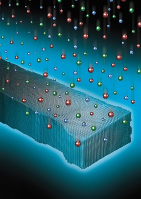 |
| Ions from a reactive plasma shape a silicon nanowire approximately 40 atoms wide. The periodic atomic arrangement is preserved up to the edge of the nanowire. CREDIT Image courtesy of V.R. Manfrinato et al., Patterning Si at the 1 nm Length Scale with Aberration-Corrected Electron-Beam Lithography: Tuning of Plasmonic Properties by Design, Adv. Funct. Mater. 2019 1903429. Wiley-VCH GmbH. Reproduced with permission. |
Abstract:
The Science
Researchers have developed an innovative technique for creating nanomaterials. These are materials only atoms wide. They draw on nanoscience to allow scientists to control their construction and behavior. The new electron beam nanofabrication technique is called plasmon engineering. It achieves unprecedented near-atomic scale control of patterning in silicon. Structures built using this approach produce record-high tuning of electro-optical properties.
Patterning silicon at the one nanometer scale: Scientists engineer materials’ electrical and optical properties with plasmon engineering
Washington, DC | Posted on August 13th, 2021The Impact
In this research, scientists used plasmon engineering to control the optical and electronic properties of silicon. The technique uses aberration-corrected electron beam lithography. This process involves using a beam of electrons to modify the surface of a material. Plasmon engineering allowed researchers to modify material at the near atomic scale. The use of “conventional” lithography means this approach could one day be applied to industrial applications. This approach will benefit researchers working on optical communications, sensing, and quantum computing.
Summary
Patterning materials at single nanometer resolution allows scientists to precisely engineer quantum confinement effects. Quantum effects are significant at these length scales and controlling the nanostructure dimensions provides direct control over electrical and optical properties. Silicon is by far the most widely-used semiconductor material in electronics, and the ability to fabricate silicone‐based devices of the smallest dimensions for novel device engineering is highly desirable. Researchers at Brookhaven’s Center for Functional Nanomaterials, a Department of Energy user facility, used aberration‐corrected electron‐beam lithography combined with dry reactive ion etching to achieve patterning of 1 nanometer features as well as surface and volume plasmon engineering in silicon. The nanofabrication technique employed here produces nanowires with a line edge roughness of 1 nanometer. In addition, this work demonstrates tuning of the silicon volume plasmon energy by 1.2 electron volt from the bulk value, which is ten times higher than previous attempts of volume plasmon engineering using lithographic methods.
Funding
This research was supported by the DOE Office of Science and used resources at the Center for Functional Nanomaterials, an Office of Science user facility at Brookhaven National Laboratory.
####
For more information, please click here
Contacts:
Michael Church
Office: 505-358-1481
Copyright © U.S. Department of Energy
If you have a comment, please Contact us.Issuers of news releases, not 7th Wave, Inc. or Nanotechnology Now, are solely responsible for the accuracy of the content.
Bookmark:


| Related Links |
| Related News Press |
News and information
![]() Quantum computer improves AI predictions April 17th, 2026
Quantum computer improves AI predictions April 17th, 2026
![]() Flexible sensor gains sensitivity under pressure April 17th, 2026
Flexible sensor gains sensitivity under pressure April 17th, 2026
![]() A reusable chip for particulate matter sensing April 17th, 2026
A reusable chip for particulate matter sensing April 17th, 2026
![]() Detecting vibrational quantum beating in the predissociation dynamics of SF6 using time-resolved photoelectron spectroscopy April 17th, 2026
Detecting vibrational quantum beating in the predissociation dynamics of SF6 using time-resolved photoelectron spectroscopy April 17th, 2026
Laboratories
![]() Researchers develop molecular qubits that communicate at telecom frequencies October 3rd, 2025
Researchers develop molecular qubits that communicate at telecom frequencies October 3rd, 2025
![]() A battery’s hopping ions remember where they’ve been: Seen in atomic detail, the seemingly smooth flow of ions through a battery’s electrolyte is surprisingly complicated February 16th, 2024
A battery’s hopping ions remember where they’ve been: Seen in atomic detail, the seemingly smooth flow of ions through a battery’s electrolyte is surprisingly complicated February 16th, 2024
Nanofabrication
![]() Self-propelled protein-based nanomotors for enhanced cancer therapy by inducing ferroptosis June 6th, 2025
Self-propelled protein-based nanomotors for enhanced cancer therapy by inducing ferroptosis June 6th, 2025
![]() Multiphoton polymerization: A promising technology for precision medicine February 28th, 2025
Multiphoton polymerization: A promising technology for precision medicine February 28th, 2025
![]() New chip opens door to AI computing at light speed February 16th, 2024
New chip opens door to AI computing at light speed February 16th, 2024
Plasmonics
![]() Unveiling the power of hot carriers in plasmonic nanostructures August 16th, 2024
Unveiling the power of hot carriers in plasmonic nanostructures August 16th, 2024
Govt.-Legislation/Regulation/Funding/Policy
![]() Quantum computer improves AI predictions April 17th, 2026
Quantum computer improves AI predictions April 17th, 2026
![]() Metasurfaces smooth light to boost magnetic sensing precision January 30th, 2026
Metasurfaces smooth light to boost magnetic sensing precision January 30th, 2026
![]() New imaging approach transforms study of bacterial biofilms August 8th, 2025
New imaging approach transforms study of bacterial biofilms August 8th, 2025
Possible Futures
![]() A fundamentally new therapeutic approach to cystic fibrosis: Nanobody repairs cellular defect April 17th, 2026
A fundamentally new therapeutic approach to cystic fibrosis: Nanobody repairs cellular defect April 17th, 2026
![]() UC Irvine physicists discover method to reverse ‘quantum scrambling’ : The work addresses the problem of information loss in quantum computing system April 17th, 2026
UC Irvine physicists discover method to reverse ‘quantum scrambling’ : The work addresses the problem of information loss in quantum computing system April 17th, 2026
Optical computing/Photonic computing
![]() ICFO researchers overcome long-standing bottleneck in single photon detection with twisted 2D materials August 8th, 2025
ICFO researchers overcome long-standing bottleneck in single photon detection with twisted 2D materials August 8th, 2025
![]() Programmable electron-induced color router array May 14th, 2025
Programmable electron-induced color router array May 14th, 2025
Discoveries
![]() Quantum computer improves AI predictions April 17th, 2026
Quantum computer improves AI predictions April 17th, 2026
![]() Flexible sensor gains sensitivity under pressure April 17th, 2026
Flexible sensor gains sensitivity under pressure April 17th, 2026
![]() A reusable chip for particulate matter sensing April 17th, 2026
A reusable chip for particulate matter sensing April 17th, 2026
![]() Detecting vibrational quantum beating in the predissociation dynamics of SF6 using time-resolved photoelectron spectroscopy April 17th, 2026
Detecting vibrational quantum beating in the predissociation dynamics of SF6 using time-resolved photoelectron spectroscopy April 17th, 2026
Materials/Metamaterials/Magnetoresistance
![]() First real-time observation of two-dimensional melting process: Researchers at Mainz University unveil new insights into magnetic vortex structures August 8th, 2025
First real-time observation of two-dimensional melting process: Researchers at Mainz University unveil new insights into magnetic vortex structures August 8th, 2025
![]() Researchers unveil a groundbreaking clay-based solution to capture carbon dioxide and combat climate change June 6th, 2025
Researchers unveil a groundbreaking clay-based solution to capture carbon dioxide and combat climate change June 6th, 2025
![]() A 1960s idea inspires NBI researchers to study hitherto inaccessible quantum states June 6th, 2025
A 1960s idea inspires NBI researchers to study hitherto inaccessible quantum states June 6th, 2025
![]() Institute for Nanoscience hosts annual proposal planning meeting May 16th, 2025
Institute for Nanoscience hosts annual proposal planning meeting May 16th, 2025
Announcements
![]() A fundamentally new therapeutic approach to cystic fibrosis: Nanobody repairs cellular defect April 17th, 2026
A fundamentally new therapeutic approach to cystic fibrosis: Nanobody repairs cellular defect April 17th, 2026
![]() UC Irvine physicists discover method to reverse ‘quantum scrambling’ : The work addresses the problem of information loss in quantum computing system April 17th, 2026
UC Irvine physicists discover method to reverse ‘quantum scrambling’ : The work addresses the problem of information loss in quantum computing system April 17th, 2026
Interviews/Book Reviews/Essays/Reports/Podcasts/Journals/White papers/Posters
![]() A fundamentally new therapeutic approach to cystic fibrosis: Nanobody repairs cellular defect April 17th, 2026
A fundamentally new therapeutic approach to cystic fibrosis: Nanobody repairs cellular defect April 17th, 2026
![]() UC Irvine physicists discover method to reverse ‘quantum scrambling’ : The work addresses the problem of information loss in quantum computing system April 17th, 2026
UC Irvine physicists discover method to reverse ‘quantum scrambling’ : The work addresses the problem of information loss in quantum computing system April 17th, 2026
Photonics/Optics/Lasers
![]() Metasurfaces smooth light to boost magnetic sensing precision January 30th, 2026
Metasurfaces smooth light to boost magnetic sensing precision January 30th, 2026
![]() From sensors to smart systems: the rise of AI-driven photonic noses January 30th, 2026
From sensors to smart systems: the rise of AI-driven photonic noses January 30th, 2026
|
|
||
|
|
||
| The latest news from around the world, FREE | ||
|
|
||
|
|
||
| Premium Products | ||
|
|
||
|
Only the news you want to read!
Learn More |
||
|
|
||
|
Full-service, expert consulting
Learn More |
||
|
|
||