Home > Press > Twisting 2D materials uncovers their superpowers: Researchers have developed a completely new method for twisting atomically thin materials, paving the way for applications of 'twistronics' based on tunable 2D materials
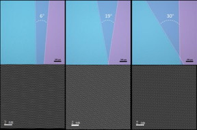 |
| The twist angle between the layers governs the crystal symmetry and can lead to a variety of interesting physical behaviours, such as unconventional superconductivity, tunnelling conductance, nonlinear optics and structural super-lubricity. CREDIT Luojun Du et al. Aalto University |
Abstract:
Two-dimensional (2D) materials, which consist of a single layer of atoms, have attracted a lot of attention since the isolation of graphene in 2004. They have unique electrical, optical, and mechanical properties, like high conductivity, flexibility and strength, which makes them promising materials for such things as lasers, photovoltaics, sensors and medical applications.
Twisting 2D materials uncovers their superpowers: Researchers have developed a completely new method for twisting atomically thin materials, paving the way for applications of 'twistronics' based on tunable 2D materials
Aalto, Finland | Posted on May 12th, 2020When a sheet of 2D material is placed over another and slightly rotated, the twist can radically change the bilayer material's properties and lead to exotic physical behaviours, such as high temperature superconductivity - exiting for electrical engineering; nonlinear optics - exciting for lasers and data transmission; and structural super-lubricity- a newly discovered mechanical property which researchers are only beginning to understand. The study of these properties has given birth to a new field of research called twistronics, so-called because it's a combination of twist and electronics.
Aalto University's researchers collaborating with international colleagues have now developed a new method for making these twisted layers on scales that are large enough to be useful, for the first time. Their new method for transferring single-atom layers of molybdenum disulfide (MoS2) allows researchers to precisely control the twist angle between layers with up to a square centimetre in area, making it record-breaking in terms of size. Controlling the interlayer twist angle on a large scale is crucial for the future practical applications of twistronics.
'Our demonstrated twist method allows us to tune the properties of stacked multilayer MoS2 structures on larger scales than ever before. The transfer method can also apply to other two-dimensional layered materials', says Dr Luojun Du from Aalto University, one of the lead authors of the work.
A significant advancement for a brand-new field of research
Since twistronics research was introduced only in 2018, basic research is still needed to understand the properties of twisted materials better before they find their ways to practical applications. The Wolf Prize in Physics, one of the most prestigious scientific awards, was awarded to Profs. Rafi Bistritzer, Pablo Jarillo-Herrero, and Allan H. MacDonald this year for their groundbreaking work on twistronics, which indicates the game-changing potential of the emerging field.
Previous research has demonstrated that it is possible to fabricate the required twist angle by transfer method or atomic force microscope tip manipulation techniques in small scales. The sample size has usually been in the order of ten-microns, less than the size of a human hair. Larger few-layer films have also been fabricated, but their interlayer twist angle is random. Now the researchers can grow large films using an epitaxial growth method and water assistant transfer method.
'Since no polymer is needed during the transfer process, the interfaces of our sample are relatively clean. With the control of twist angle and ultra-clean interfaces, we could tune the physical properties, including low-frequency interlayer modes, band structure, and optical and electrical properties', Du says.
'Indeed, the work is of great significance in guiding the future applications of twistronics based on 2D materials', adds Professor Zhipei Sun from Aalto University.
The results were published in Nature Communications.
####
For more information, please click here
Contacts:
Luojun Du
@aaltouniversity
Copyright © Aalto University
If you have a comment, please Contact us.Issuers of news releases, not 7th Wave, Inc. or Nanotechnology Now, are solely responsible for the accuracy of the content.
Bookmark:


| Related Links |
![]() M. Liao et.al., Precise control the interlayer twist angle of large scale MoS2 homostructures:
M. Liao et.al., Precise control the interlayer twist angle of large scale MoS2 homostructures:
| Related News Press |
News and information
![]() Quantum computer improves AI predictions April 17th, 2026
Quantum computer improves AI predictions April 17th, 2026
![]() Flexible sensor gains sensitivity under pressure April 17th, 2026
Flexible sensor gains sensitivity under pressure April 17th, 2026
![]() A reusable chip for particulate matter sensing April 17th, 2026
A reusable chip for particulate matter sensing April 17th, 2026
![]() Detecting vibrational quantum beating in the predissociation dynamics of SF6 using time-resolved photoelectron spectroscopy April 17th, 2026
Detecting vibrational quantum beating in the predissociation dynamics of SF6 using time-resolved photoelectron spectroscopy April 17th, 2026
2 Dimensional Materials
![]() Flexible sensor gains sensitivity under pressure April 17th, 2026
Flexible sensor gains sensitivity under pressure April 17th, 2026
Nanomedicine
![]() A fundamentally new therapeutic approach to cystic fibrosis: Nanobody repairs cellular defect April 17th, 2026
A fundamentally new therapeutic approach to cystic fibrosis: Nanobody repairs cellular defect April 17th, 2026
![]() New molecular technology targets tumors and simultaneously silences two �undruggable� cancer genes August 8th, 2025
New molecular technology targets tumors and simultaneously silences two �undruggable� cancer genes August 8th, 2025
![]() New imaging approach transforms study of bacterial biofilms August 8th, 2025
New imaging approach transforms study of bacterial biofilms August 8th, 2025
![]() Electrifying results shed light on graphene foam as a potential material for lab grown cartilage June 6th, 2025
Electrifying results shed light on graphene foam as a potential material for lab grown cartilage June 6th, 2025
Sensors
![]() Flexible sensor gains sensitivity under pressure April 17th, 2026
Flexible sensor gains sensitivity under pressure April 17th, 2026
![]() Tiny nanosheets, big leap: A new sensor detects ethanol at ultra-low levels January 30th, 2026
Tiny nanosheets, big leap: A new sensor detects ethanol at ultra-low levels January 30th, 2026
![]() From sensors to smart systems: the rise of AI-driven photonic noses January 30th, 2026
From sensors to smart systems: the rise of AI-driven photonic noses January 30th, 2026
![]() Sensors innovations for smart lithium-based batteries: advancements, opportunities, and potential challenges August 8th, 2025
Sensors innovations for smart lithium-based batteries: advancements, opportunities, and potential challenges August 8th, 2025
Discoveries
![]() Quantum computer improves AI predictions April 17th, 2026
Quantum computer improves AI predictions April 17th, 2026
![]() Flexible sensor gains sensitivity under pressure April 17th, 2026
Flexible sensor gains sensitivity under pressure April 17th, 2026
![]() A reusable chip for particulate matter sensing April 17th, 2026
A reusable chip for particulate matter sensing April 17th, 2026
![]() Detecting vibrational quantum beating in the predissociation dynamics of SF6 using time-resolved photoelectron spectroscopy April 17th, 2026
Detecting vibrational quantum beating in the predissociation dynamics of SF6 using time-resolved photoelectron spectroscopy April 17th, 2026
Announcements
![]() A fundamentally new therapeutic approach to cystic fibrosis: Nanobody repairs cellular defect April 17th, 2026
A fundamentally new therapeutic approach to cystic fibrosis: Nanobody repairs cellular defect April 17th, 2026
![]() UC Irvine physicists discover method to reverse �quantum scrambling� : The work addresses the problem of information loss in quantum computing system April 17th, 2026
UC Irvine physicists discover method to reverse �quantum scrambling� : The work addresses the problem of information loss in quantum computing system April 17th, 2026
Interviews/Book Reviews/Essays/Reports/Podcasts/Journals/White papers/Posters
![]() A fundamentally new therapeutic approach to cystic fibrosis: Nanobody repairs cellular defect April 17th, 2026
A fundamentally new therapeutic approach to cystic fibrosis: Nanobody repairs cellular defect April 17th, 2026
![]() UC Irvine physicists discover method to reverse �quantum scrambling� : The work addresses the problem of information loss in quantum computing system April 17th, 2026
UC Irvine physicists discover method to reverse �quantum scrambling� : The work addresses the problem of information loss in quantum computing system April 17th, 2026
Photonics/Optics/Lasers
![]() Metasurfaces smooth light to boost magnetic sensing precision January 30th, 2026
Metasurfaces smooth light to boost magnetic sensing precision January 30th, 2026
![]() From sensors to smart systems: the rise of AI-driven photonic noses January 30th, 2026
From sensors to smart systems: the rise of AI-driven photonic noses January 30th, 2026
Solar/Photovoltaic
![]() Spinel-type sulfide semiconductors to operate the next-generation LEDs and solar cells For solar-cell absorbers and green-LED source October 3rd, 2025
Spinel-type sulfide semiconductors to operate the next-generation LEDs and solar cells For solar-cell absorbers and green-LED source October 3rd, 2025
![]() KAIST researchers introduce new and improved, next-generation perovskite solar cell November 8th, 2024
KAIST researchers introduce new and improved, next-generation perovskite solar cell November 8th, 2024
![]() Groundbreaking precision in single-molecule optoelectronics August 16th, 2024
Groundbreaking precision in single-molecule optoelectronics August 16th, 2024
![]() Development of zinc oxide nanopagoda array photoelectrode: photoelectrochemical water-splitting hydrogen production January 12th, 2024
Development of zinc oxide nanopagoda array photoelectrode: photoelectrochemical water-splitting hydrogen production January 12th, 2024
|
|
||
|
|
||
| The latest news from around the world, FREE | ||
|
|
||
|
|
||
| Premium Products | ||
|
|
||
|
Only the news you want to read!
Learn More |
||
|
|
||
|
Full-service, expert consulting
Learn More |
||
|
|
||