Home > Press > Comprehensive review of heterogeneously integrated 2D materials
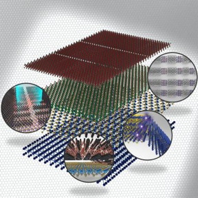 |
| Schematic illustration of the newly emerged 2D heterostructures research with various heterogeneous integration of 2D materials. CREDIT Author |
Abstract:
In a paper published in NANO, a group of researchers from Sungkyunkwan University, South Korea provide a comprehensive review of heterogeneously integrated two dimensional (2D) materials from an extensive library of atomic 2D materials with selectable material properties to open up fascinating possibilities for the design of functional novel devices.
Comprehensive review of heterogeneously integrated 2D materials
Singapore | Posted on March 6th, 2020Since the discovery of Graphene by Andre Geim and Konstantin Novoselov, 2D materials, e.g., graphene, black phosphorous (BP), transition metal dichalcogenides (TMDCs), and hexagonal boron nitride (h-BN) have attracted extensive attention due to their broad physical properties and wide range of applications to electronic and optoelectronic devices. Research on these 2D materials has matured to the point where an extensive library of atomically thin 2D materials with selectable material properties has been created and continues to grow.
By combining or stacking these 2D materials, it is possible to construct 2D heterostructures, which are built by directly stacking individual monolayers comprising different materials. Each monolayer within a 2D heterostructure is highly stable, due to strong covalent bonds between the atoms within that monolayer. However, the forces between the monolayers that keep said monolayers stacked one above the other to form the 2D heterostructure happen to be relatively weak van der Waals interactions. Due to this, each of the monolayers retains its intrinsic properties. Moreover, unlike in conventional semiconductor heterostructures where component material selection is restricted to those with similar lattice structures, the lattice mismatch requirements of stacked heterostructures can be relaxed due to the weakness of the van der Waal's forces. This means that one can combine insulating, semiconducting, or metallic 2D materials to form a single 2D heterostructure despite their different lattice structures.
When a monolayer is stacked in combination with other monolayers made out of different materials, a variety of new heterostructures with atomically thin 2D heterojunctions can be created. Heterostructures made from a particular combination of materials will have a certain set of physical characteristics depending on which materials they are made from. The unusual physical characteristics of 2D heterostructures make them suitable for use in a wide range of applications.
In this review, various 2D heterostructures are discussed along with an explanation of novel electronic and optoelectronic properties, advanced synthesis technical developments, as well as new functional applications available. It provides an understanding of the current research trends in 2D materials, so as to explore future possibilities for nanomaterial research.
###
This research was supported by the National Research Foundation of Korea funded by the Korean government (grant nos. 2013M3A6B1078873, 2015R1D1A1A09057297, 2017R1A4A1015400, and 2017R1A2A2A05001403).
Corresponding authors for this study are Euyheon Hwang ( and Sungjoo Lee ) from SKKU Advanced Institute of Nanotechnology and Department of Nano Engineering, Sungkyunkwan University.
For more insight into the research described, readers are invited to access the paper on NANO.
####
About World Scientific
World Scientific Publishing is a leading independent publisher of books and journals for the scholarly, research, professional and educational communities. The company publishes about 600 books annually and about 140 journals in various fields. World Scientific collaborates with prestigious organizations like the Nobel Foundation and US National Academies Press to bring high quality academic and professional content to researchers and academics worldwide. To find out more about World Scientific, please visit http://www.worldscientific.com .
For more information, please click here
Contacts:
Tay Yu Shan
@worldscientific
Copyright © World Scientific
If you have a comment, please Contact us.Issuers of news releases, not 7th Wave, Inc. or Nanotechnology Now, are solely responsible for the accuracy of the content.
Bookmark:


| Related Links |
| Related News Press |
News and information
![]() Quantum computer improves AI predictions April 17th, 2026
Quantum computer improves AI predictions April 17th, 2026
![]() Flexible sensor gains sensitivity under pressure April 17th, 2026
Flexible sensor gains sensitivity under pressure April 17th, 2026
![]() A reusable chip for particulate matter sensing April 17th, 2026
A reusable chip for particulate matter sensing April 17th, 2026
![]() Detecting vibrational quantum beating in the predissociation dynamics of SF6 using time-resolved photoelectron spectroscopy April 17th, 2026
Detecting vibrational quantum beating in the predissociation dynamics of SF6 using time-resolved photoelectron spectroscopy April 17th, 2026
2 Dimensional Materials
![]() Flexible sensor gains sensitivity under pressure April 17th, 2026
Flexible sensor gains sensitivity under pressure April 17th, 2026
Graphene/ Graphite
![]() Electrifying results shed light on graphene foam as a potential material for lab grown cartilage June 6th, 2025
Electrifying results shed light on graphene foam as a potential material for lab grown cartilage June 6th, 2025
![]() Breakthrough in proton barrier films using pore-free graphene oxide: Kumamoto University researchers achieve new milestone in advanced coating technologies September 13th, 2024
Breakthrough in proton barrier films using pore-free graphene oxide: Kumamoto University researchers achieve new milestone in advanced coating technologies September 13th, 2024
Possible Futures
![]() A fundamentally new therapeutic approach to cystic fibrosis: Nanobody repairs cellular defect April 17th, 2026
A fundamentally new therapeutic approach to cystic fibrosis: Nanobody repairs cellular defect April 17th, 2026
![]() UC Irvine physicists discover method to reverse �quantum scrambling� : The work addresses the problem of information loss in quantum computing system April 17th, 2026
UC Irvine physicists discover method to reverse �quantum scrambling� : The work addresses the problem of information loss in quantum computing system April 17th, 2026
Discoveries
![]() Quantum computer improves AI predictions April 17th, 2026
Quantum computer improves AI predictions April 17th, 2026
![]() Flexible sensor gains sensitivity under pressure April 17th, 2026
Flexible sensor gains sensitivity under pressure April 17th, 2026
![]() A reusable chip for particulate matter sensing April 17th, 2026
A reusable chip for particulate matter sensing April 17th, 2026
![]() Detecting vibrational quantum beating in the predissociation dynamics of SF6 using time-resolved photoelectron spectroscopy April 17th, 2026
Detecting vibrational quantum beating in the predissociation dynamics of SF6 using time-resolved photoelectron spectroscopy April 17th, 2026
Materials/Metamaterials/Magnetoresistance
![]() First real-time observation of two-dimensional melting process: Researchers at Mainz University unveil new insights into magnetic vortex structures August 8th, 2025
First real-time observation of two-dimensional melting process: Researchers at Mainz University unveil new insights into magnetic vortex structures August 8th, 2025
![]() Researchers unveil a groundbreaking clay-based solution to capture carbon dioxide and combat climate change June 6th, 2025
Researchers unveil a groundbreaking clay-based solution to capture carbon dioxide and combat climate change June 6th, 2025
![]() A 1960s idea inspires NBI researchers to study hitherto inaccessible quantum states June 6th, 2025
A 1960s idea inspires NBI researchers to study hitherto inaccessible quantum states June 6th, 2025
![]() Institute for Nanoscience hosts annual proposal planning meeting May 16th, 2025
Institute for Nanoscience hosts annual proposal planning meeting May 16th, 2025
Announcements
![]() A fundamentally new therapeutic approach to cystic fibrosis: Nanobody repairs cellular defect April 17th, 2026
A fundamentally new therapeutic approach to cystic fibrosis: Nanobody repairs cellular defect April 17th, 2026
![]() UC Irvine physicists discover method to reverse �quantum scrambling� : The work addresses the problem of information loss in quantum computing system April 17th, 2026
UC Irvine physicists discover method to reverse �quantum scrambling� : The work addresses the problem of information loss in quantum computing system April 17th, 2026
Interviews/Book Reviews/Essays/Reports/Podcasts/Journals/White papers/Posters
![]() A fundamentally new therapeutic approach to cystic fibrosis: Nanobody repairs cellular defect April 17th, 2026
A fundamentally new therapeutic approach to cystic fibrosis: Nanobody repairs cellular defect April 17th, 2026
![]() UC Irvine physicists discover method to reverse �quantum scrambling� : The work addresses the problem of information loss in quantum computing system April 17th, 2026
UC Irvine physicists discover method to reverse �quantum scrambling� : The work addresses the problem of information loss in quantum computing system April 17th, 2026
|
|
||
|
|
||
| The latest news from around the world, FREE | ||
|
|
||
|
|
||
| Premium Products | ||
|
|
||
|
Only the news you want to read!
Learn More |
||
|
|
||
|
Full-service, expert consulting
Learn More |
||
|
|
||