Home > Press > Unconventional phenomena triggered by acoustic waves in 2D materials: Opening a new way to manipulate valley transport by acoustic methods
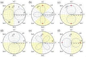 |
| Angular patterns of the x- and y- components of the conventional (a, d), warping (b, e) and Hall (c, f) electric current density. Yellow shading marks the areas of negative current (directed opposite to x- or y-axis). Red dots manifest the special angles, at which only the unconventional current flows along the x- or y-direction. CREDIT IBS |
Abstract:
Researchers at the Center for Theoretical Physics of Complex Systems (PCS), within the Institute for Basic Science (IBS, South Korea), and colleagues have reported a novel phenomenon, called Valley Acoustoelectric Effect, which takes place in 2D materials, similar to graphene. This research is published in Physical Review Letters and brings new insights to the study of valleytronics.
Unconventional phenomena triggered by acoustic waves in 2D materials: Opening a new way to manipulate valley transport by acoustic methods
Daejeon, Korea | Posted on July 23rd, 2019In acoustoelectronics, surface acoustic waves (SAWs) are employed to generate electric currents. In this study, the team of theoretical physicists modelled the propagation of SAWs in emerging 2D materials, such as single-layer molybdenum disulfide (MoS2). SAWs drag MoS2 electrons (and holes), creating an electric current with conventional and unconventional components. The latter consists of two contributions: a warping-based current and a Hall current. The first is direction-dependent, is related to the so-called valleys - electrons' local energy minima - and resembles one of the mechanisms that explains photovoltaic effects of 2D materials exposed to light. The second is due to a specific effect (Berry phase) that affects the velocity of these electrons travelling as a group and resulting in intriguing phenomena, such as anomalous and quantum Hall effects.
The team analyzed the properties of the acoustoelectric current, suggesting a way to run and measure the conventional, warping, and Hall currents independently. This allows the simultaneous use of both optical and acoustic techniques to control the propagation of charge carriers in novel 2D materials, creating new logical devices.
The researchers are interested in controlling the physical properties of these ultra-thin systems, in particular those electrons that are free to move in two dimensions, but tightly confined in the third. By curbing the parameters of the electrons, in particular their momentum, spin, and valley, it will be possible to explore technologies beyond silicon electronics. For example, MoS2 has two district valleys, which could be potentially used in the future for bit storage and processing, making it an ideal material to delve into valleytronics.
"Our theory opens a way to manipulate valley transport by acoustic methods, expanding the applicability of valleytronic effects on acoustoelectronic devices," explains Ivan Savenko, leader of the Light-Matter Interaction in Nanostructures Team at PCS.
####
For more information, please click here
Contacts:
Dahee Carol Kim
82-428-788-133
Copyright © Institute for Basic Science
If you have a comment, please Contact us.Issuers of news releases, not 7th Wave, Inc. or Nanotechnology Now, are solely responsible for the accuracy of the content.
Bookmark:


| Related Links |
| Related News Press |
News and information
![]() Quantum computer improves AI predictions April 17th, 2026
Quantum computer improves AI predictions April 17th, 2026
![]() Flexible sensor gains sensitivity under pressure April 17th, 2026
Flexible sensor gains sensitivity under pressure April 17th, 2026
![]() A reusable chip for particulate matter sensing April 17th, 2026
A reusable chip for particulate matter sensing April 17th, 2026
![]() Detecting vibrational quantum beating in the predissociation dynamics of SF6 using time-resolved photoelectron spectroscopy April 17th, 2026
Detecting vibrational quantum beating in the predissociation dynamics of SF6 using time-resolved photoelectron spectroscopy April 17th, 2026
2 Dimensional Materials
![]() Flexible sensor gains sensitivity under pressure April 17th, 2026
Flexible sensor gains sensitivity under pressure April 17th, 2026
Graphene/ Graphite
![]() Electrifying results shed light on graphene foam as a potential material for lab grown cartilage June 6th, 2025
Electrifying results shed light on graphene foam as a potential material for lab grown cartilage June 6th, 2025
![]() Breakthrough in proton barrier films using pore-free graphene oxide: Kumamoto University researchers achieve new milestone in advanced coating technologies September 13th, 2024
Breakthrough in proton barrier films using pore-free graphene oxide: Kumamoto University researchers achieve new milestone in advanced coating technologies September 13th, 2024
Possible Futures
![]() A fundamentally new therapeutic approach to cystic fibrosis: Nanobody repairs cellular defect April 17th, 2026
A fundamentally new therapeutic approach to cystic fibrosis: Nanobody repairs cellular defect April 17th, 2026
![]() UC Irvine physicists discover method to reverse �quantum scrambling� : The work addresses the problem of information loss in quantum computing system April 17th, 2026
UC Irvine physicists discover method to reverse �quantum scrambling� : The work addresses the problem of information loss in quantum computing system April 17th, 2026
Chip Technology
![]() A reusable chip for particulate matter sensing April 17th, 2026
A reusable chip for particulate matter sensing April 17th, 2026
![]() Metasurfaces smooth light to boost magnetic sensing precision January 30th, 2026
Metasurfaces smooth light to boost magnetic sensing precision January 30th, 2026
Discoveries
![]() Quantum computer improves AI predictions April 17th, 2026
Quantum computer improves AI predictions April 17th, 2026
![]() Flexible sensor gains sensitivity under pressure April 17th, 2026
Flexible sensor gains sensitivity under pressure April 17th, 2026
![]() A reusable chip for particulate matter sensing April 17th, 2026
A reusable chip for particulate matter sensing April 17th, 2026
![]() Detecting vibrational quantum beating in the predissociation dynamics of SF6 using time-resolved photoelectron spectroscopy April 17th, 2026
Detecting vibrational quantum beating in the predissociation dynamics of SF6 using time-resolved photoelectron spectroscopy April 17th, 2026
Announcements
![]() A fundamentally new therapeutic approach to cystic fibrosis: Nanobody repairs cellular defect April 17th, 2026
A fundamentally new therapeutic approach to cystic fibrosis: Nanobody repairs cellular defect April 17th, 2026
![]() UC Irvine physicists discover method to reverse �quantum scrambling� : The work addresses the problem of information loss in quantum computing system April 17th, 2026
UC Irvine physicists discover method to reverse �quantum scrambling� : The work addresses the problem of information loss in quantum computing system April 17th, 2026
Interviews/Book Reviews/Essays/Reports/Podcasts/Journals/White papers/Posters
![]() A fundamentally new therapeutic approach to cystic fibrosis: Nanobody repairs cellular defect April 17th, 2026
A fundamentally new therapeutic approach to cystic fibrosis: Nanobody repairs cellular defect April 17th, 2026
![]() UC Irvine physicists discover method to reverse �quantum scrambling� : The work addresses the problem of information loss in quantum computing system April 17th, 2026
UC Irvine physicists discover method to reverse �quantum scrambling� : The work addresses the problem of information loss in quantum computing system April 17th, 2026
|
|
||
|
|
||
| The latest news from around the world, FREE | ||
|
|
||
|
|
||
| Premium Products | ||
|
|
||
|
Only the news you want to read!
Learn More |
||
|
|
||
|
Full-service, expert consulting
Learn More |
||
|
|
||