Home > Press > Mexican scientist in the Netherlands seeks to achieve data transmission ... speed of light
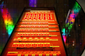 |
| Circuitos fot�nicos integrados |
Abstract:
The photonic integrated circuits could replace electronic, currently used in computers or smartphones, to make them faster and compact
In order to create effective technology that provides competitive in the market for data transmission, the mexican engineer Aura Higuera Rodriguez works in the design, manufacture and testing of dedicated optical interconnection between chips nanolasers, which ensures low power consumption and quick communication between them for sending information.
Mexican scientist in the Netherlands seeks to achieve data transmission ... speed of light
Roma, Mexico | Posted on September 20th, 2016These are devices that can measure up to 300 nanometers in length, which consume low power, ie that do not generate excessive heat such as electronic devices made from silicon. "Those who we created are capable of supporting light sources and transmit data at high speed�, explained Aura Rodriguez, a doctoral student in Photonic Integration at the Technical University of Eindhoven in the Netherlands.
A single chip can contain hundreds of thousands of devices, they can be nanolasers, receivers or transmitters. These nanolasers be adapted in optical interconnects within a single chip, for example in the central processing unit of a computer or a smartphone, the purpose is to generate quick communication between chips to send information. The next generation of devices, the era of photonics.
"When we produce is like playing with a block of modeling clay, that is what we cut and molded to create and shape the laser. We ended up forming similar blocks to the lego, who put them together forms a data transmission system that uses light to carry information at high speed�, said the Telecommunications engineer from UNAM.
Is worth highlighting that these lasers are not yet marketed in the world, because, among other things, premature state in which has not reached a performance of high efficiency, difficulty in manufacturing and handling of physical properties of materials, and processing that is delicate because they are toxic materials; however, the large telecommunications companies have already announced that they will change their mode of operation to photonics, ie invest in the development of this technology because electronics no longer be viable in the future to meet the need for data transmission more speed.
Currently the investigation is under development and continuous study. "At the moment have made a chip with nanolasers, we must now characterize and check if it works technologically and then integrate it with other functions�, explained.
Despite being technology and very expensive in Mexico may apply. "You can create designs chips using specialized software, sent to Europe to manufacture and characterize a given that the necessary equipment is not expensive as used for manufacturing laboratory. It really is possible, photonics has niche opportunity and development in Mexico, you only need to start generating cooperation and seek opportunities for projects at universities and research institutes and development to consider working with technology ".
####
For more information, please click here
Contacts:
Samara Garc�a
Copyright © AlphaGalileo
If you have a comment, please Contact us.Issuers of news releases, not 7th Wave, Inc. or Nanotechnology Now, are solely responsible for the accuracy of the content.
Bookmark:


| Related News Press |
News and information
![]() Quantum computer improves AI predictions April 17th, 2026
Quantum computer improves AI predictions April 17th, 2026
![]() Flexible sensor gains sensitivity under pressure April 17th, 2026
Flexible sensor gains sensitivity under pressure April 17th, 2026
![]() A reusable chip for particulate matter sensing April 17th, 2026
A reusable chip for particulate matter sensing April 17th, 2026
![]() Detecting vibrational quantum beating in the predissociation dynamics of SF6 using time-resolved photoelectron spectroscopy April 17th, 2026
Detecting vibrational quantum beating in the predissociation dynamics of SF6 using time-resolved photoelectron spectroscopy April 17th, 2026
Chip Technology
![]() A reusable chip for particulate matter sensing April 17th, 2026
A reusable chip for particulate matter sensing April 17th, 2026
![]() Metasurfaces smooth light to boost magnetic sensing precision January 30th, 2026
Metasurfaces smooth light to boost magnetic sensing precision January 30th, 2026
Optical computing/Photonic computing
![]() ICFO researchers overcome long-standing bottleneck in single photon detection with twisted 2D materials August 8th, 2025
ICFO researchers overcome long-standing bottleneck in single photon detection with twisted 2D materials August 8th, 2025
![]() Programmable electron-induced color router array May 14th, 2025
Programmable electron-induced color router array May 14th, 2025
Nanoelectronics
![]() Lab to industry: InSe wafer-scale breakthrough for future electronics August 8th, 2025
Lab to industry: InSe wafer-scale breakthrough for future electronics August 8th, 2025
![]() Interdisciplinary: Rice team tackles the future of semiconductors Multiferroics could be the key to ultralow-energy computing October 6th, 2023
Interdisciplinary: Rice team tackles the future of semiconductors Multiferroics could be the key to ultralow-energy computing October 6th, 2023
![]() Key element for a scalable quantum computer: Physicists from Forschungszentrum J�lich and RWTH Aachen University demonstrate electron transport on a quantum chip September 23rd, 2022
Key element for a scalable quantum computer: Physicists from Forschungszentrum J�lich and RWTH Aachen University demonstrate electron transport on a quantum chip September 23rd, 2022
![]() Reduced power consumption in semiconductor devices September 23rd, 2022
Reduced power consumption in semiconductor devices September 23rd, 2022
Discoveries
![]() Quantum computer improves AI predictions April 17th, 2026
Quantum computer improves AI predictions April 17th, 2026
![]() Flexible sensor gains sensitivity under pressure April 17th, 2026
Flexible sensor gains sensitivity under pressure April 17th, 2026
![]() A reusable chip for particulate matter sensing April 17th, 2026
A reusable chip for particulate matter sensing April 17th, 2026
![]() Detecting vibrational quantum beating in the predissociation dynamics of SF6 using time-resolved photoelectron spectroscopy April 17th, 2026
Detecting vibrational quantum beating in the predissociation dynamics of SF6 using time-resolved photoelectron spectroscopy April 17th, 2026
Announcements
![]() A fundamentally new therapeutic approach to cystic fibrosis: Nanobody repairs cellular defect April 17th, 2026
A fundamentally new therapeutic approach to cystic fibrosis: Nanobody repairs cellular defect April 17th, 2026
![]() UC Irvine physicists discover method to reverse �quantum scrambling� : The work addresses the problem of information loss in quantum computing system April 17th, 2026
UC Irvine physicists discover method to reverse �quantum scrambling� : The work addresses the problem of information loss in quantum computing system April 17th, 2026
Photonics/Optics/Lasers
![]() Metasurfaces smooth light to boost magnetic sensing precision January 30th, 2026
Metasurfaces smooth light to boost magnetic sensing precision January 30th, 2026
![]() From sensors to smart systems: the rise of AI-driven photonic noses January 30th, 2026
From sensors to smart systems: the rise of AI-driven photonic noses January 30th, 2026
|
|
||
|
|
||
| The latest news from around the world, FREE | ||
|
|
||
|
|
||
| Premium Products | ||
|
|
||
|
Only the news you want to read!
Learn More |
||
|
|
||
|
Full-service, expert consulting
Learn More |
||
|
|
||