Home > Press > Mechanical properties of nanomaterials are altered due to electric field, researchers find
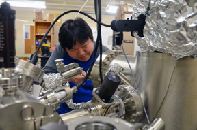 |
| TeYu Chien, a UW assistant professor in the Department of Physics and Astronomy, uses a low-temperature scanning tunneling microscope in his lab to observe nanomaterials. Chien is the lead author of a paper that appears in the journal Scientific Reports. His research determined that the electric field is responsible for the alteration of the fracture toughness of nanomaterials, which are used in state-of-the-art electronic devices. CREDIT: University of Wyoming |
Abstract:
Mechanical properties of nanomaterials can be altered due to the application of voltage, University of Wyoming researchers have discovered.
Mechanical properties of nanomaterials are altered due to electric field, researchers find
Laramie, WY | Posted on January 9th, 2016The researchers, led by TeYu Chien, a UW assistant professor in the Department of Physics and Astronomy, determined that the electric field is responsible for alterating the fracture toughness of nanomaterials, which are used in state-of-the-art electronic devices. It is the first observed evidence that the electric field changes the fracture toughness at a nanometer scale.
This finding opens the way for further investigation of nanomaterials regarding electric field-mechanical property interactions, which is extremely important for applications and fundamental research.
Chien is the lead author of a paper, titled "Built-in Electric Field Induced Mechanical Property Change at the Lanthanum Nickelate/Nb-doped Strontium Titanate Interfaces," that was recently published in Scientific Reports. Scientific Reports is an online, open-access journal from the publishers of Nature. The journal publishes scientifically valid primary research from all areas of the natural and clinical sciences.
Other researchers who contributed to the paper are from the University of Arkansas, University of Tennessee and Argonne National Laboratory in Argonne, Ill.
Chien and his research team studied the surfaces of the fractured interfaces of ceramic materials, including lanthanum nickelate and strontium titanate with a small amount of niobium. The researchers revealed that strontium titanate, within a few nanometers of the interfaces, fractured differently from the strontium titanate away from the interfaces.
The two ceramic materials were chosen because one is a metallic oxide while the other is a semiconductor. When the two types of materials come into contact with each other, an intrinsic electric field will automatically be formed in a region, known as the Schottky barrier, near the interface, Chien explains. The Schottky barrier refers to the region where an intrinsic electric field is formed at metal/semiconductor interfaces.
The intrinsic electric field at interfaces is an inevitable phenomenon whenever one material is in contact with another. The electric field effects on the mechanical properties of materials are rarely studied, especially for nanomaterials. Understanding electric field effects is extremely important for applications of nanoelectromechanical system (NEMS), which are devices, such as actuators, integrating electrical and mechanical functionalities on the nanoscale.
For NEMS materials made in nanoscale, understanding the mechanical properties affected by electric fields is crucial for full control of device performance. The observations in this study pave the way to better understand the mechanical properties of nanomaterials.
"The electric field changes the inter-atomic bond length in the crystal by pushing positively and negatively charged ions in opposite directions," Chien says. "Altering bond length changes bond strength. Hence, the mechanical properties, such as fracture toughness."
"The whole picture is this: The intrinsic electric field in the Schottky barrier was created at the interfaces. This then polarized the materials near the interfaces by changing the atomic positions in the crystal. The changed atomic positions altered the inter-atomic bond length inside the materials to change the mechanical properties near the interfaces," Chien summarizes.
####
For more information, please click here
Contacts:
TeYu Chien
307-766-6534
Copyright © University of Wyoming
If you have a comment, please Contact us.Issuers of news releases, not 7th Wave, Inc. or Nanotechnology Now, are solely responsible for the accuracy of the content.
Bookmark:


| Related Links |
| Related News Press |
News and information
![]() Quantum computer improves AI predictions April 17th, 2026
Quantum computer improves AI predictions April 17th, 2026
![]() Flexible sensor gains sensitivity under pressure April 17th, 2026
Flexible sensor gains sensitivity under pressure April 17th, 2026
![]() A reusable chip for particulate matter sensing April 17th, 2026
A reusable chip for particulate matter sensing April 17th, 2026
![]() Detecting vibrational quantum beating in the predissociation dynamics of SF6 using time-resolved photoelectron spectroscopy April 17th, 2026
Detecting vibrational quantum beating in the predissociation dynamics of SF6 using time-resolved photoelectron spectroscopy April 17th, 2026
Imaging
![]() Simple algorithm paired with standard imaging tool could predict failure in lithium metal batteries August 8th, 2025
Simple algorithm paired with standard imaging tool could predict failure in lithium metal batteries August 8th, 2025
Chip Technology
![]() A reusable chip for particulate matter sensing April 17th, 2026
A reusable chip for particulate matter sensing April 17th, 2026
![]() Metasurfaces smooth light to boost magnetic sensing precision January 30th, 2026
Metasurfaces smooth light to boost magnetic sensing precision January 30th, 2026
Nanoelectronics
![]() Lab to industry: InSe wafer-scale breakthrough for future electronics August 8th, 2025
Lab to industry: InSe wafer-scale breakthrough for future electronics August 8th, 2025
![]() Interdisciplinary: Rice team tackles the future of semiconductors Multiferroics could be the key to ultralow-energy computing October 6th, 2023
Interdisciplinary: Rice team tackles the future of semiconductors Multiferroics could be the key to ultralow-energy computing October 6th, 2023
![]() Key element for a scalable quantum computer: Physicists from Forschungszentrum J�lich and RWTH Aachen University demonstrate electron transport on a quantum chip September 23rd, 2022
Key element for a scalable quantum computer: Physicists from Forschungszentrum J�lich and RWTH Aachen University demonstrate electron transport on a quantum chip September 23rd, 2022
![]() Reduced power consumption in semiconductor devices September 23rd, 2022
Reduced power consumption in semiconductor devices September 23rd, 2022
Discoveries
![]() Quantum computer improves AI predictions April 17th, 2026
Quantum computer improves AI predictions April 17th, 2026
![]() Flexible sensor gains sensitivity under pressure April 17th, 2026
Flexible sensor gains sensitivity under pressure April 17th, 2026
![]() A reusable chip for particulate matter sensing April 17th, 2026
A reusable chip for particulate matter sensing April 17th, 2026
![]() Detecting vibrational quantum beating in the predissociation dynamics of SF6 using time-resolved photoelectron spectroscopy April 17th, 2026
Detecting vibrational quantum beating in the predissociation dynamics of SF6 using time-resolved photoelectron spectroscopy April 17th, 2026
Materials/Metamaterials/Magnetoresistance
![]() First real-time observation of two-dimensional melting process: Researchers at Mainz University unveil new insights into magnetic vortex structures August 8th, 2025
First real-time observation of two-dimensional melting process: Researchers at Mainz University unveil new insights into magnetic vortex structures August 8th, 2025
![]() Researchers unveil a groundbreaking clay-based solution to capture carbon dioxide and combat climate change June 6th, 2025
Researchers unveil a groundbreaking clay-based solution to capture carbon dioxide and combat climate change June 6th, 2025
![]() A 1960s idea inspires NBI researchers to study hitherto inaccessible quantum states June 6th, 2025
A 1960s idea inspires NBI researchers to study hitherto inaccessible quantum states June 6th, 2025
![]() Institute for Nanoscience hosts annual proposal planning meeting May 16th, 2025
Institute for Nanoscience hosts annual proposal planning meeting May 16th, 2025
Announcements
![]() A fundamentally new therapeutic approach to cystic fibrosis: Nanobody repairs cellular defect April 17th, 2026
A fundamentally new therapeutic approach to cystic fibrosis: Nanobody repairs cellular defect April 17th, 2026
![]() UC Irvine physicists discover method to reverse �quantum scrambling� : The work addresses the problem of information loss in quantum computing system April 17th, 2026
UC Irvine physicists discover method to reverse �quantum scrambling� : The work addresses the problem of information loss in quantum computing system April 17th, 2026
Interviews/Book Reviews/Essays/Reports/Podcasts/Journals/White papers/Posters
![]() A fundamentally new therapeutic approach to cystic fibrosis: Nanobody repairs cellular defect April 17th, 2026
A fundamentally new therapeutic approach to cystic fibrosis: Nanobody repairs cellular defect April 17th, 2026
![]() UC Irvine physicists discover method to reverse �quantum scrambling� : The work addresses the problem of information loss in quantum computing system April 17th, 2026
UC Irvine physicists discover method to reverse �quantum scrambling� : The work addresses the problem of information loss in quantum computing system April 17th, 2026
Tools
![]() Metasurfaces smooth light to boost magnetic sensing precision January 30th, 2026
Metasurfaces smooth light to boost magnetic sensing precision January 30th, 2026
![]() From sensors to smart systems: the rise of AI-driven photonic noses January 30th, 2026
From sensors to smart systems: the rise of AI-driven photonic noses January 30th, 2026
![]() Japan launches fully domestically produced quantum computer: Expo visitors to experience quantum computing firsthand August 8th, 2025
Japan launches fully domestically produced quantum computer: Expo visitors to experience quantum computing firsthand August 8th, 2025
|
|
||
|
|
||
| The latest news from around the world, FREE | ||
|
|
||
|
|
||
| Premium Products | ||
|
|
||
|
Only the news you want to read!
Learn More |
||
|
|
||
|
Full-service, expert consulting
Learn More |
||
|
|
||