Home > Press > Bruker Introduces Dektak XTL to Address Semiconductor Needs: New Stylus Profiler Enables Semi-Automated Measurements with Uncompromised 300mm Access
 |
Abstract:
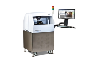
Bruker (NASDAQ: BRKR) today announced the release of the Dektak XTL Stylus Profiler, extending its industry-leading stylus profilometry capabilities to 200 and 300 millimeter semiconductor wafer fabs and next-generation touch panel manufacturers. The system provides the most cost-effective, full 300-millimeter wafer solution for characterizing thin film step heights, resist step heights, line edge roughness, CMP dishing and erosion, as well as roll off amount (ROA). The Dektak XTL combines decades of stylus innovation with new features targeting QA/QC environments to enable increased accuracy and minimal operator intervention between loading and unloading samples.
Bruker Introduces Dektak XTL to Address Semiconductor Needs: New Stylus Profiler Enables Semi-Automated Measurements with Uncompromised 300mm Access
Billerica, MA | Posted on January 14th, 2014"Bruker's Dektak XTL with a 12-inch stage is the most advanced system in its class," said Roger Lee, Integration Department Project Director for China Wafer Level CSP Co., Ltd. (WLCSP). "The system is stable and reliable, and it incorporates many powerful functionalities and ease-of-use features. Bruker's stylus profilers always lead the industry in technology, and they always meet our metrology requirements in production."
"Customers like WLCSP have been asking for a larger scale stylus measurement system to support their latest 300mm wafer factory needs with the accuracy and industry-proven repeatability of our traditional Dektak products," added Kent Heath, General Manager of Bruker's Stylus and Optical Metrology business unit. "With the Dektak XTL we have delivered on this need with its 5 nanometer repeatability, and we have built-in a new level of point-and-click automation for maximum productivity that is unrivaled in the industry. Our early access customers have been amazed by how intuitive it is to use for production and development applications."
####
About Bruker Corporation
Bruker Corporation is a leading provider of high-performance scientific instruments and solutions for molecular and materials research, as well as for industrial, diagnostics and applied analysis.
About Dektak XTL
The Dektak XTL features a small footprint with pneumatic passive isolation and a fully enclosed workstation with a wide, easily accessible interlocking door, making it suitable for demanding production floor environments. Its dual-camera architecture enables enhanced spatial awareness, and its high level of automation maximizes manufacturing throughput. Bruker�s exclusive Vision64� Advanced Production Interface (API) with pattern recognition optimizes the system for stringent QA/QC requirements and makes data collection an intuitive and repeatable process, minimizing operator-to-operator variability.
For more information, please click here
Contacts:
Stephen Hopkins
Marketing Communications
Bruker Nano Surfaces Division
T: +1 (520) 741-1044 x1022
Copyright © Bruker Corporation
If you have a comment, please Contact us.Issuers of news releases, not 7th Wave, Inc. or Nanotechnology Now, are solely responsible for the accuracy of the content.
Bookmark:


| Related News Press |
News and information
![]() Quantum computer improves AI predictions April 17th, 2026
Quantum computer improves AI predictions April 17th, 2026
![]() Flexible sensor gains sensitivity under pressure April 17th, 2026
Flexible sensor gains sensitivity under pressure April 17th, 2026
![]() A reusable chip for particulate matter sensing April 17th, 2026
A reusable chip for particulate matter sensing April 17th, 2026
![]() Detecting vibrational quantum beating in the predissociation dynamics of SF6 using time-resolved photoelectron spectroscopy April 17th, 2026
Detecting vibrational quantum beating in the predissociation dynamics of SF6 using time-resolved photoelectron spectroscopy April 17th, 2026
Thin films
![]() Tiny nanosheets, big leap: A new sensor detects ethanol at ultra-low levels January 30th, 2026
Tiny nanosheets, big leap: A new sensor detects ethanol at ultra-low levels January 30th, 2026
Display technology/LEDs/SS Lighting/OLEDs
![]() Spinel-type sulfide semiconductors to operate the next-generation LEDs and solar cells For solar-cell absorbers and green-LED source October 3rd, 2025
Spinel-type sulfide semiconductors to operate the next-generation LEDs and solar cells For solar-cell absorbers and green-LED source October 3rd, 2025
![]() Efficient and stable hybrid perovskite-organic light-emitting diodes with external quantum efficiency exceeding 40 per cent July 5th, 2024
Efficient and stable hybrid perovskite-organic light-emitting diodes with external quantum efficiency exceeding 40 per cent July 5th, 2024
Chip Technology
![]() A reusable chip for particulate matter sensing April 17th, 2026
A reusable chip for particulate matter sensing April 17th, 2026
![]() Metasurfaces smooth light to boost magnetic sensing precision January 30th, 2026
Metasurfaces smooth light to boost magnetic sensing precision January 30th, 2026
Announcements
![]() A fundamentally new therapeutic approach to cystic fibrosis: Nanobody repairs cellular defect April 17th, 2026
A fundamentally new therapeutic approach to cystic fibrosis: Nanobody repairs cellular defect April 17th, 2026
![]() UC Irvine physicists discover method to reverse �quantum scrambling� : The work addresses the problem of information loss in quantum computing system April 17th, 2026
UC Irvine physicists discover method to reverse �quantum scrambling� : The work addresses the problem of information loss in quantum computing system April 17th, 2026
Tools
![]() Metasurfaces smooth light to boost magnetic sensing precision January 30th, 2026
Metasurfaces smooth light to boost magnetic sensing precision January 30th, 2026
![]() From sensors to smart systems: the rise of AI-driven photonic noses January 30th, 2026
From sensors to smart systems: the rise of AI-driven photonic noses January 30th, 2026
![]() Japan launches fully domestically produced quantum computer: Expo visitors to experience quantum computing firsthand August 8th, 2025
Japan launches fully domestically produced quantum computer: Expo visitors to experience quantum computing firsthand August 8th, 2025
|
|
||
|
|
||
| The latest news from around the world, FREE | ||
|
|
||
|
|
||
| Premium Products | ||
|
|
||
|
Only the news you want to read!
Learn More |
||
|
|
||
|
Full-service, expert consulting
Learn More |
||
|
|
||