Home > Press > CHESS X-rays help characterize organic transistors
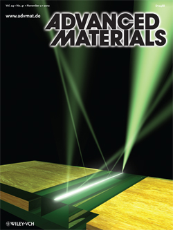 |
| Advanced Materials The cover image shows the X-ray microbeam footprint on the gate electrode of an organic transistor and scattered X-ray beams emanating from the molecular film. |
Abstract:
Plastic electronics, in which an organic material replaces silicon, hold promise for low-cost, flexible electronics. But understanding and controlling these materials' microstructures is an ongoing challenge.
CHESS X-rays help characterize organic transistors
Ithaca, NY | Posted on November 20th, 2012With the help of the D1 X-ray beamline at the Cornell High Energy Synchrotron Source (CHESS), scientists have come many steps closer to designing the perfect organic semiconductor by spatially mapping the microstructure, texture, grain sizes and grain orientations of organic semiconductor thin films.
Detlef Smilgies, senior research associate at CHESS, is co-author of an article in the Nov. 2 issue of the journal Advanced Materials (Vol. 24, No. 41), featured on the journal's cover, that describes this direct structural mapping.
The study's senior author, Aram Amassian of King Abdullah University of Science and Technology (KAUST), is a former Cornell postdoctoral associate, and the first author, Amassian's research associate Ruipeng Li, is a former visiting graduate student at CHESS; both are frequent Cornell synchrotron users.
The performance of a transistor is usually described by the mobility of its charge carriers -- the quicker the charge carriers can move through the material, the better. Charge mobility can be hampered by grain boundaries, which are the interfaces of individual grains in a crystal, either because they are misaligned or growing on different planes.
These interfaces play an important role in the texture of the crystalline organic material. A basic transistor typically has a source, where charge carriers enter; a drain, where the charge carriers exit; and a gate in the middle, which regulates the mobility of the charge carriers. In the most common architecture, the organic semiconductor is printed on a substrate pre-patterned with source and drain electrodes. The organic layer can thus form different growth planes on different parts of the substrate, and it's hard to tell fundamentally which growth planes are best to carry charges.
To shed some light on this question, the researchers used a technique called microbeam grazing incidence wide-angle X-ray scattering to probe how the organic transistor's molecular structure changed within the gate channel of the transistor, i.e., between the source and the drain electrodes. The microbeam at CHESS D1 station was obtained with an X-ray-focusing capillary -- an optical device that helps narrow the X-ray beam -- only 10 microns wide or one-fifth the width of a human hair.
This microbeam intercepted the transistors at a low angle of 2 degrees; the resulting wide-angle scattered X-rays were collected with a high-resolution camera. The scientists found that a particular growth plane that formed on the gold electrode extended up to tens of microns into the channel. Then a mix of planes occurred in the center of the channel.
When the channel width was below 20 microns, a favorable orientation prevailed, and the devices had good performance, while wider channels with mixed structures performed more poorly, with lower carrier mobility.
A chemical modification of the electrode surfaces with a fluorinated self-assembled monolayer was found to promote the formation of the favorable growth plane, which extended well into the channel. In some cases this growth plane bridged the channel entirely, significantly reducing the bottlenecks to charge transport of the untreated device.
Smilgies developed the instrumentation used in the experiment and helped with calibration and characterization of the microbeam used in the study. D1, he noted, is especially suited for in-situ studies of soft materials -- techniques that Smilgies has developed over the past 12 years at CHESS.
Oana Jurchescu and her student Jeremy Ward at Wake Forest University supplied the devices; John Anthony and Marcia Payne at the University of Kentucky provided the molecular material. CHESS is supported by the National Science Foundation and National Institutes of Health. The study was also supported by the KAUST Office of Competitive Research Funds, which funds part of the D1 beamline instrumentation.
####
For more information, please click here
Contacts:
Media Contact:
Syl Kacapyr
(607) 255-7701
Cornell Chronicle:
Anne Ju
(607) 255-9735
Copyright © Cornell University
If you have a comment, please Contact us.Issuers of news releases, not 7th Wave, Inc. or Nanotechnology Now, are solely responsible for the accuracy of the content.
Bookmark:


| Related News Press |
News and information
![]() Researchers develop molecular qubits that communicate at telecom frequencies October 3rd, 2025
Researchers develop molecular qubits that communicate at telecom frequencies October 3rd, 2025
![]() Next-generation quantum communication October 3rd, 2025
Next-generation quantum communication October 3rd, 2025
![]() "Nanoreactor" cage uses visible light for catalytic and ultra-selective cross-cycloadditions October 3rd, 2025
"Nanoreactor" cage uses visible light for catalytic and ultra-selective cross-cycloadditions October 3rd, 2025
Imaging
![]() ICFO researchers overcome long-standing bottleneck in single photon detection with twisted 2D materials August 8th, 2025
ICFO researchers overcome long-standing bottleneck in single photon detection with twisted 2D materials August 8th, 2025
![]() Simple algorithm paired with standard imaging tool could predict failure in lithium metal batteries August 8th, 2025
Simple algorithm paired with standard imaging tool could predict failure in lithium metal batteries August 8th, 2025
![]() First real-time observation of two-dimensional melting process: Researchers at Mainz University unveil new insights into magnetic vortex structures August 8th, 2025
First real-time observation of two-dimensional melting process: Researchers at Mainz University unveil new insights into magnetic vortex structures August 8th, 2025
![]() New imaging approach transforms study of bacterial biofilms August 8th, 2025
New imaging approach transforms study of bacterial biofilms August 8th, 2025
![]() Turning up the signal November 8th, 2024
Turning up the signal November 8th, 2024
Flexible Electronics
![]() Flexible electronics integrated with paper-thin structure for use in space January 17th, 2025
Flexible electronics integrated with paper-thin structure for use in space January 17th, 2025
![]() Beyond wires: Bubble technology powers next-generation electronics:New laser-based bubble printing technique creates ultra-flexible liquid metal circuits November 8th, 2024
Beyond wires: Bubble technology powers next-generation electronics:New laser-based bubble printing technique creates ultra-flexible liquid metal circuits November 8th, 2024
![]() CityU awarded invention: Soft, ultrathin photonic material cools down wearable electronic devices June 30th, 2023
CityU awarded invention: Soft, ultrathin photonic material cools down wearable electronic devices June 30th, 2023
Thin films
![]() Utilizing palladium for addressing contact issues of buried oxide thin film transistors April 5th, 2024
Utilizing palladium for addressing contact issues of buried oxide thin film transistors April 5th, 2024
![]() Understanding the mechanism of non-uniform formation of diamond film on tools: Paving the way to a dry process with less environmental impact March 24th, 2023
Understanding the mechanism of non-uniform formation of diamond film on tools: Paving the way to a dry process with less environmental impact March 24th, 2023
Govt.-Legislation/Regulation/Funding/Policy
![]() New imaging approach transforms study of bacterial biofilms August 8th, 2025
New imaging approach transforms study of bacterial biofilms August 8th, 2025
![]() Electrifying results shed light on graphene foam as a potential material for lab grown cartilage June 6th, 2025
Electrifying results shed light on graphene foam as a potential material for lab grown cartilage June 6th, 2025
![]() Institute for Nanoscience hosts annual proposal planning meeting May 16th, 2025
Institute for Nanoscience hosts annual proposal planning meeting May 16th, 2025
Chip Technology
![]() Lab to industry: InSe wafer-scale breakthrough for future electronics August 8th, 2025
Lab to industry: InSe wafer-scale breakthrough for future electronics August 8th, 2025
![]() A 1960s idea inspires NBI researchers to study hitherto inaccessible quantum states June 6th, 2025
A 1960s idea inspires NBI researchers to study hitherto inaccessible quantum states June 6th, 2025
![]() Programmable electron-induced color router array May 14th, 2025
Programmable electron-induced color router array May 14th, 2025
Self Assembly
![]() Diamond glitter: A play of colors with artificial DNA crystals May 17th, 2024
Diamond glitter: A play of colors with artificial DNA crystals May 17th, 2024
![]() Liquid crystal templated chiral nanomaterials October 14th, 2022
Liquid crystal templated chiral nanomaterials October 14th, 2022
![]() Nanoclusters self-organize into centimeter-scale hierarchical assemblies April 22nd, 2022
Nanoclusters self-organize into centimeter-scale hierarchical assemblies April 22nd, 2022
![]() Atom by atom: building precise smaller nanoparticles with templates March 4th, 2022
Atom by atom: building precise smaller nanoparticles with templates March 4th, 2022
Announcements
![]() Rice membrane extracts lithium from brines with greater speed, less waste October 3rd, 2025
Rice membrane extracts lithium from brines with greater speed, less waste October 3rd, 2025
![]() Researchers develop molecular qubits that communicate at telecom frequencies October 3rd, 2025
Researchers develop molecular qubits that communicate at telecom frequencies October 3rd, 2025
![]() Next-generation quantum communication October 3rd, 2025
Next-generation quantum communication October 3rd, 2025
![]() "Nanoreactor" cage uses visible light for catalytic and ultra-selective cross-cycloadditions October 3rd, 2025
"Nanoreactor" cage uses visible light for catalytic and ultra-selective cross-cycloadditions October 3rd, 2025
Tools
![]() Japan launches fully domestically produced quantum computer: Expo visitors to experience quantum computing firsthand August 8th, 2025
Japan launches fully domestically produced quantum computer: Expo visitors to experience quantum computing firsthand August 8th, 2025
![]() Rice researchers harness gravity to create low-cost device for rapid cell analysis February 28th, 2025
Rice researchers harness gravity to create low-cost device for rapid cell analysis February 28th, 2025
|
|
||
|
|
||
| The latest news from around the world, FREE | ||
|
|
||
|
|
||
| Premium Products | ||
|
|
||
|
Only the news you want to read!
Learn More |
||
|
|
||
|
Full-service, expert consulting
Learn More |
||
|
|
||