Home > Press > FEI Announces New Helios NanoLab 450 F1 DualBeam for Semiconductor Failure Analysis: New DualBeam from FEI delivers faster, more accurate answers for new processes, materials and complex device geometries.
 |
Abstract:
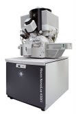
FEI (NASDAQ: FEIC) today announced its new Helios NanoLab™ 450 F1 DualBeam™ system designed to provide semiconductor manufacturers with faster, better images of their most advanced device architectures. A new STEM (scanning transmission electron microscope) detector delivers improved contrast between materials, and the new flip stage and rotating nanomanipulator support advanced preparation techniques for complex device architectures, such as finFETs and three-dimensional (3D) memory structures. Ultimately, faster, better answers cut development costs, accelerate process ramps, and get new products to market sooner.
FEI Announces New Helios NanoLab 450 F1 DualBeam for Semiconductor Failure Analysis: New DualBeam from FEI delivers faster, more accurate answers for new processes, materials and complex device geometries.
Hillsboro, OR | Posted on November 12th, 2012"The F1 combines our best new technologies into an industry leading DualBeam for semiconductor failure analysis," states Rudy Kellner, vice president and general manager of FEI's Electronics Business Unit. "The new STEM detector lets the operator know precisely when the sample is thin enough, and in many cases, the images can eliminate the need for standalone TEM analysis altogether. In fact, as samples get thinner there are advantages to working at lower beam energies where interactions with the sample are stronger. The new EasyLift nanomanipulator and flip stage let the operator maneuver the sample quickly and easily for inverted thinning, to monitor end-pointing from both sides of a section, or to section a 3D device at almost any angle."
Dual beam instruments combine an SEM (scanning electron microscope) for imaging and a FIB (focused ion beam) for milling and deposition. Dual beams also provide STEM imaging capability by adding a detector for collecting transmitted electrons below the sample. An increasingly important application of dual beam instruments is the preparation of the ultra thin samples required for TEM analysis. This need for high-resolution TEM analysis has grown dramatically in recent years as many devices structures have shrunk beyond the resolving power of SEM.
The Helios NanoLab 450 F1 is the most recent addition to FEI's line of DualBeam systems. It combines the industry's highest resolution SEM and FIB for high quality imaging and fast, precise milling and deposition, and adds capabilities specifically designed for semiconductor failure analysis applications. The new STEM detector delivers higher resolution and better material contrast. The FlipStage™ 3 quickly flips the sample between thinning and STEM viewing positions and a new rotation axis permits viewing from either side of the section. The EasyLift™ nanomanipulator provides precise motorized sample manipulation, including rotation, to support automated "lift-out" and advanced preparation procedures, such as inverted thinning. The MultiChem™ gas injector system provides unprecedented flexibility in gas assisted milling and deposition, while also cutting maintenance costs with pre-filled crucibles.
For more information, please visit: www.fei.com/helios.
####
About FEI Company
FEI (Nasdaq: FEIC) is a leading diversified scientific instruments company. It is a premier provider of electron- and ion-beam microscopes and solutions for nanoscale applications across many industries: industrial and academic materials research, life sciences, semiconductors, data storage, natural resources and more. With more than 60 years of technological innovation and leadership, FEI has set the performance standard in transmission electron microscopes (TEM), scanning electron microscopes (SEM) and DualBeams™, which combine a SEM with a focused ion beam (FIB). Headquartered in Hillsboro, Ore., USA, FEI has over 2,200 employees and sales and service operations in more than 50 countries around the world. More information can be found at: www.fei.com.
FEI Safe Harbor Statement
This news release contains forward-looking statements that include statements regarding the performance capabilities and benefits of the Helios NanoLab 450 F1 DualBeam systems. Factors that could affect these forward-looking statements include but are not limited to failure of the product or technology to perform as expected and achieve anticipated results, unexpected technology problems and challenges, changes to the technology, the inability of FEI, its suppliers or project partners to make the technological advances required for the technology to achieve anticipated results, the inability of customers to develop and deploy the expected new applications and our ability to manufacture, ship and deliver the tools or software as expected. Please also refer to our Form 10-K, Forms 10-Q, Forms 8-K and other filings with the U.S. Securities and Exchange Commission for additional information on these factors and other factors that could cause actual results to differ materially from the forward-looking statements. FEI assumes no duty to update forward-looking statements.
For more information, please click here
Contacts:
For more information contact:
Sandy Fewkes
(media contact)
MindWrite Communications, Inc
+1 408 224 4024
FEI
Fletcher Chamberlin
(investors and analysts)
Investor Relations
+1 503 726 7710
Copyright © FEI Company
If you have a comment, please Contact us.Issuers of news releases, not 7th Wave, Inc. or Nanotechnology Now, are solely responsible for the accuracy of the content.
Bookmark:


| Related News Press |
News and information
![]() Quantum computer improves AI predictions April 17th, 2026
Quantum computer improves AI predictions April 17th, 2026
![]() Flexible sensor gains sensitivity under pressure April 17th, 2026
Flexible sensor gains sensitivity under pressure April 17th, 2026
![]() A reusable chip for particulate matter sensing April 17th, 2026
A reusable chip for particulate matter sensing April 17th, 2026
![]() Detecting vibrational quantum beating in the predissociation dynamics of SF6 using time-resolved photoelectron spectroscopy April 17th, 2026
Detecting vibrational quantum beating in the predissociation dynamics of SF6 using time-resolved photoelectron spectroscopy April 17th, 2026
Imaging
![]() Simple algorithm paired with standard imaging tool could predict failure in lithium metal batteries August 8th, 2025
Simple algorithm paired with standard imaging tool could predict failure in lithium metal batteries August 8th, 2025
Chip Technology
![]() A reusable chip for particulate matter sensing April 17th, 2026
A reusable chip for particulate matter sensing April 17th, 2026
![]() Metasurfaces smooth light to boost magnetic sensing precision January 30th, 2026
Metasurfaces smooth light to boost magnetic sensing precision January 30th, 2026
Announcements
![]() A fundamentally new therapeutic approach to cystic fibrosis: Nanobody repairs cellular defect April 17th, 2026
A fundamentally new therapeutic approach to cystic fibrosis: Nanobody repairs cellular defect April 17th, 2026
![]() UC Irvine physicists discover method to reverse ‘quantum scrambling’ : The work addresses the problem of information loss in quantum computing system April 17th, 2026
UC Irvine physicists discover method to reverse ‘quantum scrambling’ : The work addresses the problem of information loss in quantum computing system April 17th, 2026
Tools
![]() Metasurfaces smooth light to boost magnetic sensing precision January 30th, 2026
Metasurfaces smooth light to boost magnetic sensing precision January 30th, 2026
![]() From sensors to smart systems: the rise of AI-driven photonic noses January 30th, 2026
From sensors to smart systems: the rise of AI-driven photonic noses January 30th, 2026
![]() Japan launches fully domestically produced quantum computer: Expo visitors to experience quantum computing firsthand August 8th, 2025
Japan launches fully domestically produced quantum computer: Expo visitors to experience quantum computing firsthand August 8th, 2025
Industrial
![]() Tiny nanosheets, big leap: A new sensor detects ethanol at ultra-low levels January 30th, 2026
Tiny nanosheets, big leap: A new sensor detects ethanol at ultra-low levels January 30th, 2026
![]() Quantum interference in molecule-surface collisions February 28th, 2025
Quantum interference in molecule-surface collisions February 28th, 2025
![]() Boron nitride nanotube fibers get real: Rice lab creates first heat-tolerant, stable fibers from wet-spinning process June 24th, 2022
Boron nitride nanotube fibers get real: Rice lab creates first heat-tolerant, stable fibers from wet-spinning process June 24th, 2022
|
|
||
|
|
||
| The latest news from around the world, FREE | ||
|
|
||
|
|
||
| Premium Products | ||
|
|
||
|
Only the news you want to read!
Learn More |
||
|
|
||
|
Full-service, expert consulting
Learn More |
||
|
|
||