Home > Press > The Noise About Graphene
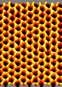 |
| This image of a single suspended sheet of graphene taken with the TEAM 0.5, at Berkeley Lab’s National Center for Electron Microscopy shows individual carbon atoms (yellow) on the honeycomb lattice. |
Abstract:
Berkeley Labs materials scientist Yuegang Zhang and colleagues at University of California, Los Angeles are moving toward more efficient devices by studying the ‘noise' in graphene nanoribbons
The Noise About Graphene
Berkeley, CA | Posted on October 18th, 2010In last week's announcement of the Nobel Prize in Physics, the Royal Swedish Academy of Sciences lauded graphene's "exceptional properties that originate from the remarkable world of quantum physics." If it weren't hot enough before, this atomically thin sheet of carbon is now officially in the global spotlight.
The promise of graphene lies in the simplicity of its structure—a ‘chicken wire' lattice of carbon atoms just one layer thick. This sheet confines electrons in one dimension, forcing them to race across a plane. Such quantum confinement results in stellar electronic, mechanical and optical properties far beyond what silicon and other traditional semiconductor materials offer. What's more, if graphene's electrons were restricted in two dimensions, like in a nanoribbon, it could greatly benefit logic switching devices—the basis for computation units in today's computer chips.
Now, Berkeley Labs materials scientist Yuegang Zhang and colleagues at University of California, Los Angeles are moving toward more efficient devices by studying the ‘noise' in such graphene nanoribbons—one-dimensional strips of graphene with nanometer-scale widths.
"Atomically-thin graphene nanoribbons have provided an excellent platform for us to reveal the strong correlation between conductance fluctuation and the quantized electronic structures of quasi-one-dimensional systems," says Zhang, a staff scientist in the Inorganic Nanostructures Facility at the Molecular Foundry. "This method should have much broader use to understand quantum transport phenomena in other nanoelectronic or molecular devices."
Zhang and colleagues previously reported ways of fabricating films of graphene (1) and revealing low-frequency signal-to-noise ratios for graphene devices on a silica substrate (2). In the current study, the team made graphene nanoribbons using a nanowire mask-based fabrication technique. By measuring the conductance fluctuation, or ‘noise' of electrons in graphene nanoribbons, the researchers directly probed the effect of quantum confinement in these structures. Their findings map the electronic band structure of these graphene nanoribbons using a robust electrical probing method. This method can be further applied to a wide array of nanoscale materials, including graphene-based electronic devices.
"It amazes us to observe such a clear correlation between the noise and the band structure of these graphene nanomaterials," says lead author Guangyu Xu, a physicist at University of California, Los Angeles. "This work adds strong support to the quasi-one-dimensional subband formation in graphene nanoribbons, in which our method turns out to be much more robust than conductance measurement."
A paper reporting this research titled, "Enhanced conductance fluctuation by quantum confinement effect in graphene nanoribbons," appears in Nano Letters and is available to subscribers online . Co-authoring the paper with Zhang and Xu were Carlos Torres, Jr., Emil Song, Jianshi Tang, Jingwei Bai, Xiangfeng Duan and Kang L. Wang.
Portions of this work at the Molecular Foundry were supported by DOE's Office of Science.
The Molecular Foundry is one of the five DOE Nanoscale Science Research Centers (NSRCs), national user facilities for interdisciplinary research at the nanoscale, supported by the DOE Office of Science. Together the NSRCs comprise a suite of complementary facilities that provide researchers with state-of-the-art capabilities to fabricate, process, characterize and model nanoscale materials, and constitute the largest infrastructure investment of the National Nanotechnology Initiative. The NSRCs are located at DOE's Argonne, Brookhaven, Lawrence Berkeley, Oak Ridge and Sandia and Los Alamos National Laboratories. For more information about the DOE NSRCs, please visit nano.energy.gov.
(1) newscenter.lbl.gov/feature-stories/2010/04/08/graphene-films/
(2) newscenter.lbl.gov/news-releases/2010/08/06/noise-in-graphene/
####
About Lawrence Berkeley National Laboratory
Berkeley Lab is a U.S. Department of Energy national laboratory located in Berkeley, California. It conducts unclassified scientific research and is managed by the University of California.
Visit our website at www.lbl.gov
For more information, please click here
Contacts:
Aditi Risbud
(510) 486-4861
Copyright © Berkeley Lab
If you have a comment, please Contact us.Issuers of news releases, not 7th Wave, Inc. or Nanotechnology Now, are solely responsible for the accuracy of the content.
Bookmark:


| Related News Press |
News and information
![]() Quantum computer improves AI predictions April 17th, 2026
Quantum computer improves AI predictions April 17th, 2026
![]() Flexible sensor gains sensitivity under pressure April 17th, 2026
Flexible sensor gains sensitivity under pressure April 17th, 2026
![]() A reusable chip for particulate matter sensing April 17th, 2026
A reusable chip for particulate matter sensing April 17th, 2026
![]() Detecting vibrational quantum beating in the predissociation dynamics of SF6 using time-resolved photoelectron spectroscopy April 17th, 2026
Detecting vibrational quantum beating in the predissociation dynamics of SF6 using time-resolved photoelectron spectroscopy April 17th, 2026
Govt.-Legislation/Regulation/Funding/Policy
![]() Quantum computer improves AI predictions April 17th, 2026
Quantum computer improves AI predictions April 17th, 2026
![]() Metasurfaces smooth light to boost magnetic sensing precision January 30th, 2026
Metasurfaces smooth light to boost magnetic sensing precision January 30th, 2026
![]() New imaging approach transforms study of bacterial biofilms August 8th, 2025
New imaging approach transforms study of bacterial biofilms August 8th, 2025
Possible Futures
![]() A fundamentally new therapeutic approach to cystic fibrosis: Nanobody repairs cellular defect April 17th, 2026
A fundamentally new therapeutic approach to cystic fibrosis: Nanobody repairs cellular defect April 17th, 2026
![]() UC Irvine physicists discover method to reverse ‘quantum scrambling’ : The work addresses the problem of information loss in quantum computing system April 17th, 2026
UC Irvine physicists discover method to reverse ‘quantum scrambling’ : The work addresses the problem of information loss in quantum computing system April 17th, 2026
Academic/Education
![]() Rice University launches Rice Synthetic Biology Institute to improve lives January 12th, 2024
Rice University launches Rice Synthetic Biology Institute to improve lives January 12th, 2024
![]() Multi-institution, $4.6 million NSF grant to fund nanotechnology training September 9th, 2022
Multi-institution, $4.6 million NSF grant to fund nanotechnology training September 9th, 2022
Chip Technology
![]() A reusable chip for particulate matter sensing April 17th, 2026
A reusable chip for particulate matter sensing April 17th, 2026
![]() Metasurfaces smooth light to boost magnetic sensing precision January 30th, 2026
Metasurfaces smooth light to boost magnetic sensing precision January 30th, 2026
Nanoelectronics
![]() Lab to industry: InSe wafer-scale breakthrough for future electronics August 8th, 2025
Lab to industry: InSe wafer-scale breakthrough for future electronics August 8th, 2025
![]() Interdisciplinary: Rice team tackles the future of semiconductors Multiferroics could be the key to ultralow-energy computing October 6th, 2023
Interdisciplinary: Rice team tackles the future of semiconductors Multiferroics could be the key to ultralow-energy computing October 6th, 2023
![]() Key element for a scalable quantum computer: Physicists from Forschungszentrum Jülich and RWTH Aachen University demonstrate electron transport on a quantum chip September 23rd, 2022
Key element for a scalable quantum computer: Physicists from Forschungszentrum Jülich and RWTH Aachen University demonstrate electron transport on a quantum chip September 23rd, 2022
![]() Reduced power consumption in semiconductor devices September 23rd, 2022
Reduced power consumption in semiconductor devices September 23rd, 2022
Announcements
![]() A fundamentally new therapeutic approach to cystic fibrosis: Nanobody repairs cellular defect April 17th, 2026
A fundamentally new therapeutic approach to cystic fibrosis: Nanobody repairs cellular defect April 17th, 2026
![]() UC Irvine physicists discover method to reverse ‘quantum scrambling’ : The work addresses the problem of information loss in quantum computing system April 17th, 2026
UC Irvine physicists discover method to reverse ‘quantum scrambling’ : The work addresses the problem of information loss in quantum computing system April 17th, 2026
Quantum nanoscience
![]() Beyond silicon: Electronics at the scale of a single molecule January 30th, 2026
Beyond silicon: Electronics at the scale of a single molecule January 30th, 2026
![]() MXene nanomaterials enter a new dimension Multilayer nanomaterial: MXene flakes created at Drexel University show new promise as 1D scrolls January 30th, 2026
MXene nanomaterials enter a new dimension Multilayer nanomaterial: MXene flakes created at Drexel University show new promise as 1D scrolls January 30th, 2026
![]() ICFO researchers overcome long-standing bottleneck in single photon detection with twisted 2D materials August 8th, 2025
ICFO researchers overcome long-standing bottleneck in single photon detection with twisted 2D materials August 8th, 2025
|
|
||
|
|
||
| The latest news from around the world, FREE | ||
|
|
||
|
|
||
| Premium Products | ||
|
|
||
|
Only the news you want to read!
Learn More |
||
|
|
||
|
Full-service, expert consulting
Learn More |
||
|
|
||