Home > Press > IBM Research Creates World's Smallest 3D Map; Brings Low-Cost, Ease of Use to Creation of Nanoscale Objects
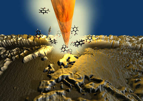 |
| 3D rendered image showing a heated nanoscale silicon tip, borrowed from atomic force microscopy that is chiselling away material from a substrate to create a nanoscale 3D map of the world. As reported in the scientific journal Advanced Materials, IBM Researchers used this new nanopatterning technique to create the smallest map of the world in 3D, measuring only 22 by 11 micrometers was “written” – on a polymer - at this size 1000 world maps could fit on a grain of salt. In the relief, one thousand meters of altitude correspond to roughly eight nanometers (nm). It is composed of 500,000 pixels, each measuring 20 nm2 and was created in only 2 minutes and 23 seconds. (Image courtesy of Advanced Materials). |
Abstract:
IBM (NYSE: IBM) scientists have created a 3D map of the earth so small that 1,000 of them could fit on one grain of salt.* The scientists accomplished this through a new, breakthrough technique that uses a tiny, silicon tip with a sharp apex — 100,000 times smaller than a sharpened pencil — to create patterns and structures as small as 15 nanometers at greatly reduced cost and complexity. This patterning technique opens new prospects for developing nanosized objects in fields such as electronics, future chip technology, medicine, life sciences, and optoelectronics.
IBM Research Creates World's Smallest 3D Map; Brings Low-Cost, Ease of Use to Creation of Nanoscale Objects
Zurich & San Jose, CA | Posted on April 24th, 2010To demonstrate the technique's unique capability, the team created several 3D and 2D patterns, using different materials for each one as reported in the scientific journals Science and Advanced Materials:
* A 25-nanometer-high 3D replica of the Matterhorn, a famous Alpine mountain that soars 4,478 m (14,692 ft) high, was created in molecular glass, representing a scale of 1:5 billion.**
* Complete 3D map of the world measuring only 22 by 11 micrometers was "written" on a polymer. At this size, 1,000 world maps could fit on a grain of salt. In the relief, one thousand meters of altitude correspond to roughly eight nanometers (nm). It is composed of 500,000 pixels, each measuring 20 nm2, and was created in only 2 minutes and 23 seconds.
* 2D nano-sized IBM logo was etched 400-nm-deep into silicon, demonstrating the viability of the technique for typical nanofabrication applications.
* 2D high-resolution 15-nm dense line patterning.
The science behind the technique
The core component of the new technique, which was developed by a team of IBM scientists, is a tiny, very sharp silicon tip measuring 500 nanometers in length and only a few nanometers at its apex.
"Advances in nanotechnology are intimately linked to the existence of high-quality methods and tools for producing nanoscale patterns and objects on surfaces," explains physicist Dr. Armin Knoll of IBM Research - Zurich. "With its broad functionality and unique 3D patterning capability, this nanotip-based patterning methodology is a powerful tool for generating very small structures."
The tip, similar to the kind used in atomic force microscopes, is attached to a bendable cantilever that controllably scans the surface of the substrate material with the accuracy of one nanometer—a millionth of a millimeter. By applying heat and force, the nano-sized tip can remove substrate material based on predefined patterns, thus operating like a "nanomilling" machine with ultra-high precision.
Similar to using a milling machine, more material can be removed to create complex 3D structures with nanometer precision by modulating the force or by readdressing individual spots. To create the 3D replica of the Matterhorn, for example, 120 individual layers of material were successively removed from the molecular glass substrate.
Comparing to e-beam lithography
The new IBM technique achieves resolutions as high as 15 nanometers—with a potential of going even smaller. Using existing methods such as e-beam lithography,*** it is becoming increasingly challenging to fabricate patterns at resolutions below 30 nanometers, where the technical limitations of that method are reached.
What's more, compared to expensive e-beam-lithography tools that require several processing steps and equipment that can easily fill a laboratory, the tool created by IBM scientists—which can sit on a tabletop—promises improved and extended capabilities at very high resolutions, but at one-fifth to one tenth of the cost and with far less complexity.
Yet another advantage of the nanotip-based technique is the ability to assess the pattern directly by using the same tip to create an image of the written structures, as the IBM scientists demonstrated in their experiments.
Potential applications range from the fast prototyping of nano-sized devices for future computer chips to the production of well defined micron-sized optical elements like aspheric lenses and lens-arrays for optoelectronics and on-chip optical communication.
Materials breakthrough
In the two publications, the scientists describe their novel 3D-nanopatterning methodology for two very distinct and promising types of substrate materials: a polymer called polyphthalaldehyde and a molecular glass similar to substrate materials used in conventional nanofabrication techniques, so-called resists. Identifying these two materials was a key factor for the breakthrough performance and reliability of the technique.
In their search for suitable and efficient substrate materials, the scientists concentrated on organic materials that could be used as resists, thereby following the same philosophy as used for today's semiconductor technology, which is important for further integration.
"The material was a 'make it or break it' issue," explains Jim Hedrick, scientist at IBM Research - Almaden. "We had to find and synthesize materials which form mechanically tough glasses and yet can be easily thermally decomposed into non-reactive volatile units."
The molecular glass that was used in the Matterhorn experiment consists of snow-flake-like molecules, measuring about one nanometer and having an almost spherical shape. At a tip temperature above 330 degrees C (626 degrees F), the hydrogen bonds that hold the molecules together break, allowing the molecular parts to become mobile and to escape from the surface. A particular strength of the material is that the patterned molecular glass can be transferred by means of conventional etching techniques to, for example, silicon, which is common in the semiconductor industry. Molecular glass was first proposed in the late 1990s by Mitsuru Ueda of Yamagata University, Japan, for use as high-resolution photoresists and was thereafter developed by Chris Ober of Cornell University.
The nanosized 3D world map was created in a polymer called polyphthalaldehyde, a polymer originally developed by IBM Fellow Hiroshi Ito in the 1980s. Exposed to substantially elevated temperatures, the components of this chain-like organic molecule unzip and fall into volatile pieces. A self-amplified reaction causes the molecule to decompose and then accelerates the entire patterning process by being even faster than the mechanical motion of the tip.
IBM and nanotechnology
IBM has been a pioneer in nanoscience and nanotechnology ever since the development of the scanning tunneling microscope (STM) in 1981 by IBM Fellows Gerd Binnig and Heinrich Rohrer. For this invention, which made it possible to image individual atoms and later on to manipulate them, Binnig and Rohrer were awarded the Nobel Prize in Physics in 1986. The atomic force microscope, an offspring of the STM, was invented by Binnig in 1986. The STM is widely regarded as the instrument that opened the door to the nanoworld.
In fact it was 20 years ago this month that IBM Fellow Don Eigler reported the first controlled movement of individual atoms, famously using a scanning tunneling microscope to spell out the letters "I B M" with 35 xenon atoms.
These historic breakthroughs laid a solid foundation for IBM's continued research in nanoscience.
Contributing to this rich history for years to come, a new world-class collaborative nanoscale research lab is currently under construction on the campus of IBM Research - Zurich. This state-of-the-art nanotech center, which will open next year, is part of a strategic partnership in nanotechnology between IBM Research and ETH Zurich, one of Europe's leading technical universities.
* Taking 0.3 mm as the average size of a grain of salt, 1000 maps would span the diameter.
** One nanometer in the vertical pattern corresponds to 57 altitude meters.
*** This method selectively exposes a surface to a beam of electrons, thereby creating patterns in a film, called a resist. The resist serves as a template for transferring the pattern to various materials, for example silicon, by means of etching. It is one of the most versatile and mature methods used today, but it is very costly and complex.
asmarterplanet.com
Scientific publications
The scientific paper entitled "Nanoscale 3D Patterning of Molecular Resists by Scanning Probes" by D. Pires, J. L. Hedrick, A. De Silva, J. Frommer, B. Gotsmann, H. Wolf, M. Despont, U. Duerig and A. W. Knoll was published by Science on the Science Express website on April 22, 2010, DOI: 10.1126/science. 1187851
The scientific paper entitled "Probe-based 3-D Nanolithography Using Self-Amplified Depolymerization Polymers" by A. Knoll, D. Pires, O. Coulembier, P. Dubois, J. L. Hedrick, J. Frommer and U. Duerig was published in Advanced Materials, advanced online publication on April 23, 2010, DOI: 10.1002/adma. 200904386
(with video)
####
For more information, please click here
Contacts:
J. Michael Loughran
IBM Media Relations (U.S.)
914-945-1613
Christopher P. Sciacca
IBM Media Relations (Switzerland)
+41 44 724 84 43
Copyright © IBM
If you have a comment, please Contact us.Issuers of news releases, not 7th Wave, Inc. or Nanotechnology Now, are solely responsible for the accuracy of the content.
Bookmark:


| Related News Press |
News and information
![]() Quantum computer improves AI predictions April 17th, 2026
Quantum computer improves AI predictions April 17th, 2026
![]() Flexible sensor gains sensitivity under pressure April 17th, 2026
Flexible sensor gains sensitivity under pressure April 17th, 2026
![]() A reusable chip for particulate matter sensing April 17th, 2026
A reusable chip for particulate matter sensing April 17th, 2026
![]() Detecting vibrational quantum beating in the predissociation dynamics of SF6 using time-resolved photoelectron spectroscopy April 17th, 2026
Detecting vibrational quantum beating in the predissociation dynamics of SF6 using time-resolved photoelectron spectroscopy April 17th, 2026
Physics
![]() UC Irvine physicists discover method to reverse ‘quantum scrambling’ : The work addresses the problem of information loss in quantum computing system April 17th, 2026
UC Irvine physicists discover method to reverse ‘quantum scrambling’ : The work addresses the problem of information loss in quantum computing system April 17th, 2026
![]() Quantum computers simulate fundamental physics: shedding light on the building blocks of nature June 6th, 2025
Quantum computers simulate fundamental physics: shedding light on the building blocks of nature June 6th, 2025
![]() A 1960s idea inspires NBI researchers to study hitherto inaccessible quantum states June 6th, 2025
A 1960s idea inspires NBI researchers to study hitherto inaccessible quantum states June 6th, 2025
Videos/Movies
![]() ICFO researchers overcome long-standing bottleneck in single photon detection with twisted 2D materials August 8th, 2025
ICFO researchers overcome long-standing bottleneck in single photon detection with twisted 2D materials August 8th, 2025
Possible Futures
![]() A fundamentally new therapeutic approach to cystic fibrosis: Nanobody repairs cellular defect April 17th, 2026
A fundamentally new therapeutic approach to cystic fibrosis: Nanobody repairs cellular defect April 17th, 2026
![]() UC Irvine physicists discover method to reverse ‘quantum scrambling’ : The work addresses the problem of information loss in quantum computing system April 17th, 2026
UC Irvine physicists discover method to reverse ‘quantum scrambling’ : The work addresses the problem of information loss in quantum computing system April 17th, 2026
Chip Technology
![]() A reusable chip for particulate matter sensing April 17th, 2026
A reusable chip for particulate matter sensing April 17th, 2026
![]() Metasurfaces smooth light to boost magnetic sensing precision January 30th, 2026
Metasurfaces smooth light to boost magnetic sensing precision January 30th, 2026
Nanomedicine
![]() A fundamentally new therapeutic approach to cystic fibrosis: Nanobody repairs cellular defect April 17th, 2026
A fundamentally new therapeutic approach to cystic fibrosis: Nanobody repairs cellular defect April 17th, 2026
![]() New molecular technology targets tumors and simultaneously silences two ‘undruggable’ cancer genes August 8th, 2025
New molecular technology targets tumors and simultaneously silences two ‘undruggable’ cancer genes August 8th, 2025
![]() New imaging approach transforms study of bacterial biofilms August 8th, 2025
New imaging approach transforms study of bacterial biofilms August 8th, 2025
![]() Electrifying results shed light on graphene foam as a potential material for lab grown cartilage June 6th, 2025
Electrifying results shed light on graphene foam as a potential material for lab grown cartilage June 6th, 2025
Nanoelectronics
![]() Lab to industry: InSe wafer-scale breakthrough for future electronics August 8th, 2025
Lab to industry: InSe wafer-scale breakthrough for future electronics August 8th, 2025
![]() Interdisciplinary: Rice team tackles the future of semiconductors Multiferroics could be the key to ultralow-energy computing October 6th, 2023
Interdisciplinary: Rice team tackles the future of semiconductors Multiferroics could be the key to ultralow-energy computing October 6th, 2023
![]() Key element for a scalable quantum computer: Physicists from Forschungszentrum Jülich and RWTH Aachen University demonstrate electron transport on a quantum chip September 23rd, 2022
Key element for a scalable quantum computer: Physicists from Forschungszentrum Jülich and RWTH Aachen University demonstrate electron transport on a quantum chip September 23rd, 2022
![]() Reduced power consumption in semiconductor devices September 23rd, 2022
Reduced power consumption in semiconductor devices September 23rd, 2022
Announcements
![]() A fundamentally new therapeutic approach to cystic fibrosis: Nanobody repairs cellular defect April 17th, 2026
A fundamentally new therapeutic approach to cystic fibrosis: Nanobody repairs cellular defect April 17th, 2026
![]() UC Irvine physicists discover method to reverse ‘quantum scrambling’ : The work addresses the problem of information loss in quantum computing system April 17th, 2026
UC Irvine physicists discover method to reverse ‘quantum scrambling’ : The work addresses the problem of information loss in quantum computing system April 17th, 2026
Tools
![]() Metasurfaces smooth light to boost magnetic sensing precision January 30th, 2026
Metasurfaces smooth light to boost magnetic sensing precision January 30th, 2026
![]() From sensors to smart systems: the rise of AI-driven photonic noses January 30th, 2026
From sensors to smart systems: the rise of AI-driven photonic noses January 30th, 2026
![]() Japan launches fully domestically produced quantum computer: Expo visitors to experience quantum computing firsthand August 8th, 2025
Japan launches fully domestically produced quantum computer: Expo visitors to experience quantum computing firsthand August 8th, 2025
Nanobiotechnology
![]() A fundamentally new therapeutic approach to cystic fibrosis: Nanobody repairs cellular defect April 17th, 2026
A fundamentally new therapeutic approach to cystic fibrosis: Nanobody repairs cellular defect April 17th, 2026
![]() New molecular technology targets tumors and simultaneously silences two ‘undruggable’ cancer genes August 8th, 2025
New molecular technology targets tumors and simultaneously silences two ‘undruggable’ cancer genes August 8th, 2025
![]() New imaging approach transforms study of bacterial biofilms August 8th, 2025
New imaging approach transforms study of bacterial biofilms August 8th, 2025
![]() Electrifying results shed light on graphene foam as a potential material for lab grown cartilage June 6th, 2025
Electrifying results shed light on graphene foam as a potential material for lab grown cartilage June 6th, 2025
Photonics/Optics/Lasers
![]() Metasurfaces smooth light to boost magnetic sensing precision January 30th, 2026
Metasurfaces smooth light to boost magnetic sensing precision January 30th, 2026
![]() From sensors to smart systems: the rise of AI-driven photonic noses January 30th, 2026
From sensors to smart systems: the rise of AI-driven photonic noses January 30th, 2026
|
|
||
|
|
||
| The latest news from around the world, FREE | ||
|
|
||
|
|
||
| Premium Products | ||
|
|
||
|
Only the news you want to read!
Learn More |
||
|
|
||
|
Full-service, expert consulting
Learn More |
||
|
|
||