Home > Press > Fabrication of Large-area Mosaic Wafers of Single Crystal Diamond
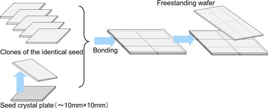 |
| Figure 1 : Production process of a mosaic large-area wafer |
Abstract:
Towards the realization of diamond electronic devices
* Development of a technology for fabrication of bonded (mosaic) wafers, which is necessary to realize the applications of diamond to devices
* Successful prototyping of 1-inch wafers using this new technology
* Planning to bring the wafers into practical use within one year, as they would lead to applications of diamonds in electronic devices
Fabrication of Large-area Mosaic Wafers of Single Crystal Diamond
Japan | Posted on March 25th, 2010Summary
Hideaki Yamada (Research Scientist) and Akiyoshi Chayahara (Leader), Diamond Wafer Team, The Diamond Research Center (Director: Naoji Fujimori) of the National Institute of Advanced Industrial Science and Technology (AIST) (President: Tamotsu Nomakuchi) have developed a technology for manufacturing inch-size large-area wafers of single crystal diamond.
Since diamond has excellent properties including high hardness, high thermal conductivity, high transmittance in a wide wavelength region, a wide band gap, and chemical stability, they have possible applications in semiconductor devices, electron-emitting devices, and biosensors, as well as in tools and optical parts. Among the applications of diamonds in electronics, diamond power devices which would surpass silicon or silicon carbide power devices are expected. Applications of diamond power devices in control modules for electric cars and industrial equipment may lead to considerable energy saving. However, the technology for manufacturing inch-size wafers of single crystal diamond is indispensable for the application of diamond devices in electronics.
Earlier, AIST developed the technology for synthesizing large single crystals of diamond and successfully synthesized a 10-mm2 wafer. This was enabled by the establishment of the "Direct Wafer-making technique," by which laminar single crystals and seed crystals of diamond can be separated. This technology is expected to enable low-cost production of unprecedentedly large single crystals.
AIST has produced several laminae of diamond single crystals with uniform properties by adopting the Direct Wafer-making technique, and bonded these laminae together to obtain a large-area wafer. We established the bonding technology to achieve a better bonding than that achieved by adopting the conventional technologies and applied our bonding technology to successfully produce single crystal diamond wafers with a large area of approximately 1 inch2.
The results of this research will be presented at the 57th Spring Meeting, 2010, of the Japan Society of Applied Physics to be held at Shonan Campus, Tokai University on March 17-20, 2010.
Social Background for Research
Since diamond has various useful properties such as high hardness, high thermal conductivity, high transmittance in a wide wavelength region, low dielectric constant, and chemical stability, the applications of diamond in various devices are anticipated. There are particularly high expectations for realizing the applications of diamond in semiconductors. Production of inch-size single crystal wafers is necessary for the practical application of diamond to semiconductors, in order to utilize semiconductor production processes.
Single crystals of natural diamond that have sizes of several millimeters or more are very rare, and it is almost impossible to increase crystal size to the order of an inch during a synthesis under ultrahigh pressure. Several attempts have been made to grow diamonds by chemical vapor deposition (CVD) because there are relatively few restrictions involved in this method; however, crystal growth cannot be easily maintained over a long period, and the technology for the mass production of large-area wafers of single crystal diamond has not yet been realized.
History of Research
Since 2003, the Diamond Research Center of AIST has been engaged in research on the synthesis of large single crystals of diamond by using the microwave plasma CVD method. The center established the conditions under which high-quality crystals can be rapidly synthesized, and successfully synthesized a 1-carat diamond single crystal in 2004. Although processing diamonds into wafers has been considered difficult, we developed the original Direct Wafer-making technique in which ion implantation and electrochemical etching are carried out; thus, laminar single crystals with arbitrary thickness can be mass-produced. Further, we synthesized 10 mm2 wafers of single crystal diamond in 2007 by achieving successive increases in crystal size.
We developed a technology to fabricate large-area bonded (mosaic) wafers of single crystalline diamond by bonding several laminar diamond single crystals produced from the same seed crystal so that larger-area wafers can be produced.
Diamond crystals can be synthesized only under extremely well-maintained and limited technical conditions. It was unclear whether large-area single crystals can be synthesized while maintaining the quality in the existing equipment. AIST improved the conditions for the synthesis of large-area diamond single crystals by using a plasma simulation method, and concluded that it is possible to achieve uniform growth on the surface of 1 inch.
Details of Research
In the past, many attempts have been made to obtain large single crystals of diamond; several research institutes have focused on the technologies to bond several single crystals and to fabricate mosaic single crystal wafers. However, it was extremely difficult to align the crystal orientation when bonding the separately synthesized crystals and the growth of polycrystals or graphite at the boundary between crystals inhibited bonding. Further, these substrates had very small sizes of 5 mm or less.
As shown in Fig. 1, the characteristic of the production technology developed by AIST is that several laminar diamond single crystals are synthesized from one seed crystal; these single crystals are bonded to obtain a large-area mosaic single crystal wafer. Since the laminar diamond single crystals are grown from one seed crystal, they are almost identical and have uniform properties and the same crystal orientation. A large-area single crystal wafer is fabricated by bonding such laminar crystals, and thus, it is possible to bond these crystals without abnormal crystal growth at the boundary between crystals and without difficulties in bonding.
In the large-area single crystal wafers fabricated using this technology, the bonding between crystals is smoother and denser than those produced by the conventional methods. Therefore, polishing processes and the Direct Wafer-making technique can be applied to the mosaic wafers. Thus, it is possible to mass manufacture the desired quantity of large-area substrates by using the fabricated large-area single crystal wafers as the seed crystal. We also demonstrated that the Direct Wafer-making technique, which is a processing technology for separation of the laminar single crystal and the seed crystal, can be applied to large-area 1-inch2 diamond crystals.
In this study, the area of 1 inch2 was covered by six laminar crystals prepared using a 10-mm2 seed crystal, which we have already synthesized. Mosaic wafers can be obtained by combining larger single crystals if the size of the seed crystals can be increased.
As described above, AIST has developed a technology which easily fabricates large-area mosaic wafers of single crystal diamond by bonding several laminar diamond single crystals synthesized from the same seed crystal. It would be possible to mass-manufacture large-area single crystal wafers by using this large-area wafer as the seed crystal and by applying the Direct Wafer-making technique.
Future Schedule
The inch-size wafers of single crystal diamond that have been produced will be examined further to realize practical use of the wafers within one year.
To realize the applications of diamonds in semiconductor devices, larger wafers will be necessary. We will conduct research to realize further increase in the sizes of wafers. In the future, AIST will try to develop uniform 2-inch wafers by improving the equipments and techniques for growing and processing. We will also improve the crystal quality to achieve the level required for device production.
####
About National Institute of Advanced Industrial Science and Technology (AIST)
National Institute of Advanced Industrial Science and Technology (AIST), led by President Dr. Nomakuchi, is not a government institution, although funded by Japanese government to a large extent. The present AIST is a rather new research organization established in 2001, however, AIST and its predecessor organizations have been contributing to society through continuous advancement in technologies and support of Japanese industries since 1876.
Headquarters of AIST are located in Tsukuba and Tokyo. AIST has over 50 autonomous research units in various innovative research fields, and the units are located at 9 research bases and several sites (smaller than research bases) of AIST all over Japan. About 2500 research scientists (about 2000 with tenure) and well over 3000 visiting scientists, post doctoral fellows and students are working at AIST. About 700 permanent administrative personnel and many temporary staff supports research works of AIST.
For more information, please click here
Copyright © AIST
If you have a comment, please Contact us.Issuers of news releases, not 7th Wave, Inc. or Nanotechnology Now, are solely responsible for the accuracy of the content.
Bookmark:


| Related News Press |
News and information
![]() Quantum computer improves AI predictions April 17th, 2026
Quantum computer improves AI predictions April 17th, 2026
![]() Flexible sensor gains sensitivity under pressure April 17th, 2026
Flexible sensor gains sensitivity under pressure April 17th, 2026
![]() A reusable chip for particulate matter sensing April 17th, 2026
A reusable chip for particulate matter sensing April 17th, 2026
![]() Detecting vibrational quantum beating in the predissociation dynamics of SF6 using time-resolved photoelectron spectroscopy April 17th, 2026
Detecting vibrational quantum beating in the predissociation dynamics of SF6 using time-resolved photoelectron spectroscopy April 17th, 2026
Possible Futures
![]() A fundamentally new therapeutic approach to cystic fibrosis: Nanobody repairs cellular defect April 17th, 2026
A fundamentally new therapeutic approach to cystic fibrosis: Nanobody repairs cellular defect April 17th, 2026
![]() UC Irvine physicists discover method to reverse �quantum scrambling� : The work addresses the problem of information loss in quantum computing system April 17th, 2026
UC Irvine physicists discover method to reverse �quantum scrambling� : The work addresses the problem of information loss in quantum computing system April 17th, 2026
Chip Technology
![]() A reusable chip for particulate matter sensing April 17th, 2026
A reusable chip for particulate matter sensing April 17th, 2026
![]() Metasurfaces smooth light to boost magnetic sensing precision January 30th, 2026
Metasurfaces smooth light to boost magnetic sensing precision January 30th, 2026
Nanoelectronics
![]() Lab to industry: InSe wafer-scale breakthrough for future electronics August 8th, 2025
Lab to industry: InSe wafer-scale breakthrough for future electronics August 8th, 2025
![]() Interdisciplinary: Rice team tackles the future of semiconductors Multiferroics could be the key to ultralow-energy computing October 6th, 2023
Interdisciplinary: Rice team tackles the future of semiconductors Multiferroics could be the key to ultralow-energy computing October 6th, 2023
![]() Key element for a scalable quantum computer: Physicists from Forschungszentrum J�lich and RWTH Aachen University demonstrate electron transport on a quantum chip September 23rd, 2022
Key element for a scalable quantum computer: Physicists from Forschungszentrum J�lich and RWTH Aachen University demonstrate electron transport on a quantum chip September 23rd, 2022
![]() Reduced power consumption in semiconductor devices September 23rd, 2022
Reduced power consumption in semiconductor devices September 23rd, 2022
Announcements
![]() A fundamentally new therapeutic approach to cystic fibrosis: Nanobody repairs cellular defect April 17th, 2026
A fundamentally new therapeutic approach to cystic fibrosis: Nanobody repairs cellular defect April 17th, 2026
![]() UC Irvine physicists discover method to reverse �quantum scrambling� : The work addresses the problem of information loss in quantum computing system April 17th, 2026
UC Irvine physicists discover method to reverse �quantum scrambling� : The work addresses the problem of information loss in quantum computing system April 17th, 2026
|
|
||
|
|
||
| The latest news from around the world, FREE | ||
|
|
||
|
|
||
| Premium Products | ||
|
|
||
|
Only the news you want to read!
Learn More |
||
|
|
||
|
Full-service, expert consulting
Learn More |
||
|
|
||