Home > Press > Graphene electronics
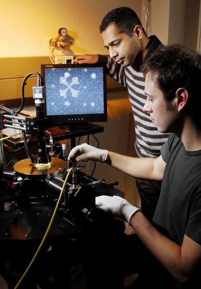 |
| Researchers Raghunath Murali and graduate student Kevin Brenner(front) perform electrical measurements on a graphene sample under high vacuum in a cryogenic probe station. Credit: Georgia Tech Photo: Gary Meek |
Abstract:
Single-step technique produces both p-type and n-type doping for future graphene devices
Graphene electronics
Atlanta, GA | Posted on February 11th, 2010A simple one-step process that produces both n-type and p-type doping of large-area graphene surfaces could facilitate use of the promising material for future electronic devices. The doping technique can also be used to increase conductivity in graphene nanoribbons used for interconnects.
By applying a commercially-available spin-on-glass (SOG) material to graphene and then exposing it to electron-beam radiation, researchers at the Georgia Institute of Technology created both types of doping by simply varying the exposure time. Higher levels of e-beam energy produced p-type areas, while lower levels produced n-type areas.
The technique was used to fabricate high-resolution p-n junctions. When properly passivated, the doping created by the SOG is expected to remain indefinitely in the graphene sheets studied by the researchers.
"This is an enabling step toward making possible complementary metal oxide graphene transistors," said Raghunath Murali, a senior research engineer in Georgia Tech's Nanotechnology Research Center.
A paper describing the technique appears this week in the journal Applied Physics Letters. The research was supported by the Semiconductor Research Corporation and the Defense Advanced Research Projects Agency (DARPA) through the Interconnect Focus Center.
In the new doping process, Murali and graduate student Kevin Brenner begin by removing flakes of graphene one to four layers thick from a block of graphite. They place the material onto a surface of oxidized silicon, then fabricate a four-point contact device.
Next, they spin on films of hydrogen silsesquoxane (HSQ), then cure certain portions of the resulting thin film using electron beam radiation. The technique provides precise control over the amount of radiation and where it is applied to the graphene, with higher levels of energy corresponding to more cross-linking of the HSQ.
"We gave varying doses of electron-beam radiation and then studied how it influenced the properties of carriers in the graphene lattice," Murali said. "The e-beam gave us a fine range of control that could be valuable for fabricating nanoscale devices. We can use an electron beam with a diameter of four or five nanometers that allows very precise doping patterns."
Electronic measurements showed that a graphene p-n junction created by the new technique had large energy separations, indicating strong doping effects, he added.
Researchers elsewhere have demonstrated graphene doping using a variety of processes including soaking the material in various solutions and exposing it to a variety of gases. The Georgia Tech process is believed to be the first to provide both electron and hole doping from a single dopant material.
Doping processes used for graphene are likely to be significantly different from those established for silicon use, Murali said. In silicon, the doping step substitutes atoms of a different material for silicon atoms in the material's lattice.
In the new single-step process for graphene, the doping is believed to introduce atoms of hydrogen and oxygen in the vicinity of the carbon lattice. The oxygen and hydrogen don't replace carbon atoms, but instead occupy locations atop the lattice structure.
"Energy applied to the SOG breaks chemical bonds and releases hydrogen and oxygen which bond with the carbon lattice," Murali said. "A high e-beam energy converts the whole SOG structure to more of a network, and then you have more oxygen than hydrogen, resulting in a p-type doping."
In volume manufacturing, the electron beam radiation would likely be replaced by a conventional lithography process, Murali said. Varying the reflectance or transmission of the mask set would control the amount of radiation reaching the SOG, and that would determine whether n-type or p-type areas are created.
"Making everything in a single step would avoid some of the expensive lithography steps," he said. "Gray-scale lithography would allow fine control of doping across the entire surface of the wafer."
For doping bulk areas such as interconnects that do not require patterning, the researchers simply coat the area with HSQ and expose it to a plasma source. The technique can make the nanoribbons up to 10 times more conductive than untreated graphene.
Because HSQ is already familiar to the microelectronics industry, the one-step approach to doping could help integrate graphene into existing processes, avoiding a disruption of the massive semiconductor design and fabrication system, Murali noted.
Over the past two years, researchers in the Nanotechnology Research Center had observed changes caused by application of HSQ during electrical testing. Only recently did they take a closer look at what was happening to understand how to take advantage of the phenomenon.
For the future, they'd like to better understand how the process works and whether other polymers might provide better results.
"We need to have a better understanding of how to control this process because variability is one of the issues that must be controlled to make manufacturing feasible," Murali explained. "We are trying to identify other polymers that may provide better control or stronger doping levels."
####
About Georgia Institute of Technology
The Georgia Institute of Technology is one of the nation's top research universities, distinguished by its commitment to improving the human condition through advanced science and technology.
Georgia Tech's campus occupies 400 acres in the heart of the city of Atlanta, where 20,000 undergraduate and graduate students receive a focused, technologically based education.
For more information, please click here
Contacts:
John Toon
404-894-6986
Copyright © Georgia Institute of Technology
If you have a comment, please Contact us.Issuers of news releases, not 7th Wave, Inc. or Nanotechnology Now, are solely responsible for the accuracy of the content.
Bookmark:


| Related News Press |
News and information
![]() Quantum computer improves AI predictions April 17th, 2026
Quantum computer improves AI predictions April 17th, 2026
![]() Flexible sensor gains sensitivity under pressure April 17th, 2026
Flexible sensor gains sensitivity under pressure April 17th, 2026
![]() A reusable chip for particulate matter sensing April 17th, 2026
A reusable chip for particulate matter sensing April 17th, 2026
![]() Detecting vibrational quantum beating in the predissociation dynamics of SF6 using time-resolved photoelectron spectroscopy April 17th, 2026
Detecting vibrational quantum beating in the predissociation dynamics of SF6 using time-resolved photoelectron spectroscopy April 17th, 2026
Govt.-Legislation/Regulation/Funding/Policy
![]() Quantum computer improves AI predictions April 17th, 2026
Quantum computer improves AI predictions April 17th, 2026
![]() Metasurfaces smooth light to boost magnetic sensing precision January 30th, 2026
Metasurfaces smooth light to boost magnetic sensing precision January 30th, 2026
![]() New imaging approach transforms study of bacterial biofilms August 8th, 2025
New imaging approach transforms study of bacterial biofilms August 8th, 2025
Possible Futures
![]() A fundamentally new therapeutic approach to cystic fibrosis: Nanobody repairs cellular defect April 17th, 2026
A fundamentally new therapeutic approach to cystic fibrosis: Nanobody repairs cellular defect April 17th, 2026
![]() UC Irvine physicists discover method to reverse �quantum scrambling� : The work addresses the problem of information loss in quantum computing system April 17th, 2026
UC Irvine physicists discover method to reverse �quantum scrambling� : The work addresses the problem of information loss in quantum computing system April 17th, 2026
Chip Technology
![]() A reusable chip for particulate matter sensing April 17th, 2026
A reusable chip for particulate matter sensing April 17th, 2026
![]() Metasurfaces smooth light to boost magnetic sensing precision January 30th, 2026
Metasurfaces smooth light to boost magnetic sensing precision January 30th, 2026
Nanoelectronics
![]() Lab to industry: InSe wafer-scale breakthrough for future electronics August 8th, 2025
Lab to industry: InSe wafer-scale breakthrough for future electronics August 8th, 2025
![]() Interdisciplinary: Rice team tackles the future of semiconductors Multiferroics could be the key to ultralow-energy computing October 6th, 2023
Interdisciplinary: Rice team tackles the future of semiconductors Multiferroics could be the key to ultralow-energy computing October 6th, 2023
![]() Key element for a scalable quantum computer: Physicists from Forschungszentrum J�lich and RWTH Aachen University demonstrate electron transport on a quantum chip September 23rd, 2022
Key element for a scalable quantum computer: Physicists from Forschungszentrum J�lich and RWTH Aachen University demonstrate electron transport on a quantum chip September 23rd, 2022
![]() Reduced power consumption in semiconductor devices September 23rd, 2022
Reduced power consumption in semiconductor devices September 23rd, 2022
Announcements
![]() A fundamentally new therapeutic approach to cystic fibrosis: Nanobody repairs cellular defect April 17th, 2026
A fundamentally new therapeutic approach to cystic fibrosis: Nanobody repairs cellular defect April 17th, 2026
![]() UC Irvine physicists discover method to reverse �quantum scrambling� : The work addresses the problem of information loss in quantum computing system April 17th, 2026
UC Irvine physicists discover method to reverse �quantum scrambling� : The work addresses the problem of information loss in quantum computing system April 17th, 2026
|
|
||
|
|
||
| The latest news from around the world, FREE | ||
|
|
||
|
|
||
| Premium Products | ||
|
|
||
|
Only the news you want to read!
Learn More |
||
|
|
||
|
Full-service, expert consulting
Learn More |
||
|
|
||