Home > Press > World's smallest semiconductor laser heralds new era in optical science
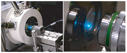 |
| A bright point of light from a single plasmon laser emanates from the optical setup used by UC Berkeley researchers (enlarged closeup at right). These semiconductor lasers � the world's smallest � are extremely efficient, so the small amount of scattered light is clearly visible, even in ambient room lighting. Camera saturation of the bright laser light gives the impression of a larger spot. (Courtesy of Xiang Zhang Lab/UC Berkeley) |
Abstract:
Researchers at the University of California, Berkeley, have reached a new milestone in laser physics by creating the world's smallest semiconductor laser, capable of generating visible light in a space smaller than a single protein molecule.
World's smallest semiconductor laser heralds new era in optical science
Berkeley, CA | Posted on September 1st, 2009This breakthrough, described in an advanced online publication of the journal Nature on Sunday, Aug. 30, breaks new ground in the field of optics. The UC Berkeley team not only successfully squeezed light into such a tight space, but found a novel way to keep that light energy from dissipating as it moved along, thereby achieving laser action.
"This work shatters traditional notions of laser limits, and makes a major advance toward applications in the biomedical, communications and computing fields," said Xiang Zhang, director at UC Berkeley of a National Science Foundation (NSF) Nanoscale Science and Engineering Center, and head of the research team behind this work
The achievement helps enable the development of such innovations as nanolasers that can probe, manipulate and characterize DNA molecules; optics-based telecommunications many times faster than current technology; and optical computing in which light replaces electronic circuitry with a corresponding leap in speed and processing power.
While it is traditionally accepted that an electromagnetic wave - including laser light - cannot be focused beyond the size of half its wavelength, research teams around the world have found a way to compress light down to dozens of nanometers by binding it to the electrons that oscillate collectively at the surface of metals. This interaction between light and oscillating electrons is known as surface plasmons.
Scientists have been racing to construct surface plasmon lasers that can sustain and utilize these tiny optical excitations. However, the resistance inherent in metals causes these surface plasmons to dissipate almost immediately after being generated, posing a critical challenge to achieving the buildup of the electromagnetic field necessary for lasing.
Zhang, a professor of mechanical engineering, and his research team took a novel approach to stem the loss of light energy by pairing a cadmium sulfide nanowire - 1,000 times thinner than a human hair - with a silver surface separated by an insulating gap of only 5 nanometers, the size of a single protein molecule. In this structure, the gap region stores light within an area 20 times smaller than its wavelength. Because light energy is largely stored in this tiny non-metallic gap, loss is significantly diminished.
With the loss finally under control through this unique "hybrid" design, the researchers could then work on amplifying the light.
"When you are working at such small scales, you do not have much space to play around with," said Rupert Oulton, the research associate in Zhang's lab who first theorized this approach last year and the study's co-lead author. "In our design, the nanowire acts as both a confinement mechanism and an amplifier. It's pulling double duty."
Trapping and sustaining light in radically tight quarters creates such extreme conditions that the very interaction of light and matter is strongly altered, the study authors explained. An increase in the spontaneous emission rate of light is a telltale sign of this altered interaction; in this study, the researchers measured a six-fold increase in the spontaneous emission rate of light in a gap size of 5 nanometers.
Recently, researchers from Norfolk State University reported lasing action of gold spheres in a dye-filled, glasslike shell immersed in a solution. The dye coupled to the gold spheres could generate surface plasmons when exposed to light.
The UC Berkeley researchers used semiconductor materials and fabrication technologies that are commonly employed in modern electronics manufacturing. By engineering hybrid surface plasmons in the tiny gap between semiconductors and metals, they were able to sustain the strongly confined light long enough that its oscillations stabilized into the coherent state that is a key characteristic of a laser.
"What is particularly exciting about the plasmonic lasers we demonstrated here is that they are solid state and fully compatible with semiconductor manufacturing, so they can be electrically pumped and fully integrated at chip-scale," said Volker Sorger, a Ph.D. student in Zhang's lab and study co-lead author.
"Plasmon lasers represent an exciting class of coherent light sources capable of extremely small confinement," said Zhang. "This work can bridge the worlds of electronics and optics at truly molecular length scales."
Scientists hope to eventually shrink light down to the size of an electron's wavelength, which is about a nanometer, or one-billionth of a meter, so that the two can work together on equal footing.
"The advantages of optics over electronics are multifold," added Thomas Zentgraf, a post-doctoral fellow in Zhang's lab and another co-lead author of the Nature paper. "For example, devices will be more power efficient at the same time they offer increased speed or bandwidth."
In addition to the three co-lead authors, other co-authors of the paper are Renmin Ma and Lun Dai from Peking University, and Christopher Gladden and Guy Bartal from Zhang's research group.
This work is supported by the U.S. Air Force Office of Scientific Research and the NSF.
####
About University of California, Berkeley
We teach - educating students at all levels, from undergraduate to the most advanced graduate level. Undergraduate programs are available to all eligible California high-school graduates and community college transfer students who wish to attend the University of California.
Instructional programs at the undergraduate level transmit knowledge and skills to students. At the graduate level, students experience with their instructors the processes of developing and testing new hypotheses and fresh interpretations of knowledge. Education for professional careers, grounded in understanding of relevant sciences, literature and research methods, provides individuals with the tools to continue intellectual development over a lifetime and to contribute to the needs of a changing society.
Through our academic programs, UC helps create an educated workforce that keeps the California economy competitive. And, through University Extension, with a half-million enrollments annually, UC provides continuing education for Californians to improve their job skills and enhance the quality of their lives.
For more information, please click here
Contacts:
Science/Environment/Health/ Technology
Robert Sanders
(510) 643-6998
Copyright © University of California, Berkeley
If you have a comment, please Contact us.Issuers of news releases, not 7th Wave, Inc. or Nanotechnology Now, are solely responsible for the accuracy of the content.
Bookmark:


| Related News Press |
News and information
![]() Quantum computer improves AI predictions April 17th, 2026
Quantum computer improves AI predictions April 17th, 2026
![]() Flexible sensor gains sensitivity under pressure April 17th, 2026
Flexible sensor gains sensitivity under pressure April 17th, 2026
![]() A reusable chip for particulate matter sensing April 17th, 2026
A reusable chip for particulate matter sensing April 17th, 2026
![]() Detecting vibrational quantum beating in the predissociation dynamics of SF6 using time-resolved photoelectron spectroscopy April 17th, 2026
Detecting vibrational quantum beating in the predissociation dynamics of SF6 using time-resolved photoelectron spectroscopy April 17th, 2026
Govt.-Legislation/Regulation/Funding/Policy
![]() Quantum computer improves AI predictions April 17th, 2026
Quantum computer improves AI predictions April 17th, 2026
![]() Metasurfaces smooth light to boost magnetic sensing precision January 30th, 2026
Metasurfaces smooth light to boost magnetic sensing precision January 30th, 2026
![]() New imaging approach transforms study of bacterial biofilms August 8th, 2025
New imaging approach transforms study of bacterial biofilms August 8th, 2025
Nanomedicine
![]() A fundamentally new therapeutic approach to cystic fibrosis: Nanobody repairs cellular defect April 17th, 2026
A fundamentally new therapeutic approach to cystic fibrosis: Nanobody repairs cellular defect April 17th, 2026
![]() New molecular technology targets tumors and simultaneously silences two �undruggable� cancer genes August 8th, 2025
New molecular technology targets tumors and simultaneously silences two �undruggable� cancer genes August 8th, 2025
![]() New imaging approach transforms study of bacterial biofilms August 8th, 2025
New imaging approach transforms study of bacterial biofilms August 8th, 2025
![]() Electrifying results shed light on graphene foam as a potential material for lab grown cartilage June 6th, 2025
Electrifying results shed light on graphene foam as a potential material for lab grown cartilage June 6th, 2025
Optical computing/Photonic computing
![]() ICFO researchers overcome long-standing bottleneck in single photon detection with twisted 2D materials August 8th, 2025
ICFO researchers overcome long-standing bottleneck in single photon detection with twisted 2D materials August 8th, 2025
![]() Programmable electron-induced color router array May 14th, 2025
Programmable electron-induced color router array May 14th, 2025
Nanoelectronics
![]() Lab to industry: InSe wafer-scale breakthrough for future electronics August 8th, 2025
Lab to industry: InSe wafer-scale breakthrough for future electronics August 8th, 2025
![]() Interdisciplinary: Rice team tackles the future of semiconductors Multiferroics could be the key to ultralow-energy computing October 6th, 2023
Interdisciplinary: Rice team tackles the future of semiconductors Multiferroics could be the key to ultralow-energy computing October 6th, 2023
![]() Key element for a scalable quantum computer: Physicists from Forschungszentrum J�lich and RWTH Aachen University demonstrate electron transport on a quantum chip September 23rd, 2022
Key element for a scalable quantum computer: Physicists from Forschungszentrum J�lich and RWTH Aachen University demonstrate electron transport on a quantum chip September 23rd, 2022
![]() Reduced power consumption in semiconductor devices September 23rd, 2022
Reduced power consumption in semiconductor devices September 23rd, 2022
Discoveries
![]() Quantum computer improves AI predictions April 17th, 2026
Quantum computer improves AI predictions April 17th, 2026
![]() Flexible sensor gains sensitivity under pressure April 17th, 2026
Flexible sensor gains sensitivity under pressure April 17th, 2026
![]() A reusable chip for particulate matter sensing April 17th, 2026
A reusable chip for particulate matter sensing April 17th, 2026
![]() Detecting vibrational quantum beating in the predissociation dynamics of SF6 using time-resolved photoelectron spectroscopy April 17th, 2026
Detecting vibrational quantum beating in the predissociation dynamics of SF6 using time-resolved photoelectron spectroscopy April 17th, 2026
Announcements
![]() A fundamentally new therapeutic approach to cystic fibrosis: Nanobody repairs cellular defect April 17th, 2026
A fundamentally new therapeutic approach to cystic fibrosis: Nanobody repairs cellular defect April 17th, 2026
![]() UC Irvine physicists discover method to reverse �quantum scrambling� : The work addresses the problem of information loss in quantum computing system April 17th, 2026
UC Irvine physicists discover method to reverse �quantum scrambling� : The work addresses the problem of information loss in quantum computing system April 17th, 2026
Nanobiotechnology
![]() A fundamentally new therapeutic approach to cystic fibrosis: Nanobody repairs cellular defect April 17th, 2026
A fundamentally new therapeutic approach to cystic fibrosis: Nanobody repairs cellular defect April 17th, 2026
![]() New molecular technology targets tumors and simultaneously silences two �undruggable� cancer genes August 8th, 2025
New molecular technology targets tumors and simultaneously silences two �undruggable� cancer genes August 8th, 2025
![]() New imaging approach transforms study of bacterial biofilms August 8th, 2025
New imaging approach transforms study of bacterial biofilms August 8th, 2025
![]() Electrifying results shed light on graphene foam as a potential material for lab grown cartilage June 6th, 2025
Electrifying results shed light on graphene foam as a potential material for lab grown cartilage June 6th, 2025
Photonics/Optics/Lasers
![]() Metasurfaces smooth light to boost magnetic sensing precision January 30th, 2026
Metasurfaces smooth light to boost magnetic sensing precision January 30th, 2026
![]() From sensors to smart systems: the rise of AI-driven photonic noses January 30th, 2026
From sensors to smart systems: the rise of AI-driven photonic noses January 30th, 2026
|
|
||
|
|
||
| The latest news from around the world, FREE | ||
|
|
||
|
|
||
| Premium Products | ||
|
|
||
|
Only the news you want to read!
Learn More |
||
|
|
||
|
Full-service, expert consulting
Learn More |
||
|
|
||