Home > Press > Graphene Shows Promise for Future IC Interconnects
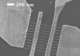 |
| Image: Raghunath Murali This scanning electron microscope image shows graphene nanoribbons that are 22 nanometers wide between the middle electrode pair. |
Abstract:
The unique properties of thin layers of graphite - known as graphene - make the material attractive for a wide range of potential electronic devices. Researchers have now experimentally demonstrated the potential for another graphene application: replacing copper for interconnects in future generations of integrated circuits.
Graphene Shows Promise for Future IC Interconnects
Atlanta, GA | Posted on June 4th, 2009In a paper published in the June 2009 issue of the IEEE journal Electron Device Letters, researchers at the Georgia Institute of Technology report detailed analysis of resistivity in graphene nanoribbon interconnects as narrow as 18 nanometers.
The results suggest that graphene could out-perform copper for use as on-chip interconnects - tiny wires that are used to connect transistors and other devices on integrated circuits. Use of graphene for these interconnects could help extend the long run of performance improvements for silicon-based integrated circuit technology.
"As you make copper interconnects narrower and narrower, the resistivity increases as the true nanoscale properties of the material become apparent," said Raghunath Murali, a research engineer in Georgia Tech's Microelectronics Research Center. "Our experimental demonstration of graphene nanowire interconnects on the scale of 20 nanometers shows that their performance is comparable to even the most optimistic projections for copper interconnects at that scale. Under real-world conditions, our graphene interconnects probably already out-perform copper at this size scale."
Beyond resistivity improvement, graphene interconnects would offer higher electron mobility, better thermal conductivity, higher mechanical strength and reduced capacitance coupling between adjacent wires.
"Resistivity is normally independent of the dimension - a property inherent to the material," Murali noted. "But as you get into the nanometer-scale domain, the grain sizes of the copper become important and conductance is affected by scattering at the grain boundaries and at the side walls. These add up to increased resistivity, which nearly doubles as the interconnect sizes shrink to 30 nanometers."
The research was supported by the Interconnect Focus Center, which is one of the Semiconductor Research Corporation/DARPA Focus Centers, and the Nanoelectronics Research Initiative through the INDEX Center.
Murali and collaborators Kevin Brenner, Yinxiao Yang, Thomas Beck and James Meindl studied the electrical properties of graphene layers that had been taken from a block of pure graphite. They believe the attractive properties will ultimately also be measured in graphene fabricated using other techniques, such as growth on silicon carbide, which now produces graphene of lower quality but has the potential for achieving higher quality.
Because graphene can be patterned using conventional microelectronics processes, the transition from copper could be made without integrating a new manufacturing technique into circuit fabrication.
"We are optimistic about being able to use graphene in manufactured systems because researchers can already grow layers of it in the lab," Murali noted. "There will be challenges in integrating graphene with silicon, but those will be overcome. Except for using a different material, everything we would need to produce graphene interconnects is already well known and established."
Experimentally, the researchers began with flakes of multi-layered graphene removed from a graphite block and placed onto an oxidized silicon substrate. They used electron beam lithography to construct four electrode contacts on the graphene, then used lithography to fabricate devices consisting of parallel nanoribbons of widths ranging between 18 and 52 nanometers. The three-dimensional resistivity of the nanoribbons on 18 different devices was then measured using standard analytical techniques at room temperature.
The best of the graphene nanoribbons showed conductivity equal to that predicted for copper interconnects of the same size. Because the comparisons were between non-optimized graphene and optimistic estimates for copper, they suggest that performance of the new material will ultimately surpass that of the traditional interconnect material, Murali said.
"Even graphene samples of moderate quality show excellent properties," he explained. "We are not using very high levels of optimization or especially clean processes. With our straightforward processing, we are getting graphene interconnects that are essentially comparable to copper. If we do this more optimally, the performance should surpass copper."
Though one of graphene's key properties is reported to be ballistic transport - meaning electrons can flow through it without resistance - the material's actual conductance is limited by factors that include scattering from impurities, line-edge roughness and from substrate phonons - vibrations in the substrate lattice.
Use of graphene interconnects could help facilitate continuing increases in integrated circuit performance once features sizes drop to approximately 20 nanometers, which could happen in the next five years, Murali said. At that scale, the increased resistance of copper interconnects could offset performance increases, meaning that without other improvements, higher density wouldn't produce faster integrated circuits.
"This is not a roadblock to achieving scaling from one generation to the next, but it is a roadblock to achieving increased performance," he said. "Dimensional scaling could continue, but because we would be giving up so much in terms of resistivity, we wouldn't get a performance advantage from that. That's the problem we hope to solve by switching to a different materials system for interconnects."
####
For more information, please click here
Contacts:
John Toon
404-894-6986
or
Abby Vogel
404-385-3364
Copyright © Newswise
If you have a comment, please Contact us.Issuers of news releases, not 7th Wave, Inc. or Nanotechnology Now, are solely responsible for the accuracy of the content.
Bookmark:


| Related News Press |
News and information
![]() Quantum computer improves AI predictions April 17th, 2026
Quantum computer improves AI predictions April 17th, 2026
![]() Flexible sensor gains sensitivity under pressure April 17th, 2026
Flexible sensor gains sensitivity under pressure April 17th, 2026
![]() A reusable chip for particulate matter sensing April 17th, 2026
A reusable chip for particulate matter sensing April 17th, 2026
![]() Detecting vibrational quantum beating in the predissociation dynamics of SF6 using time-resolved photoelectron spectroscopy April 17th, 2026
Detecting vibrational quantum beating in the predissociation dynamics of SF6 using time-resolved photoelectron spectroscopy April 17th, 2026
Chip Technology
![]() A reusable chip for particulate matter sensing April 17th, 2026
A reusable chip for particulate matter sensing April 17th, 2026
![]() Metasurfaces smooth light to boost magnetic sensing precision January 30th, 2026
Metasurfaces smooth light to boost magnetic sensing precision January 30th, 2026
Nanoelectronics
![]() Lab to industry: InSe wafer-scale breakthrough for future electronics August 8th, 2025
Lab to industry: InSe wafer-scale breakthrough for future electronics August 8th, 2025
![]() Interdisciplinary: Rice team tackles the future of semiconductors Multiferroics could be the key to ultralow-energy computing October 6th, 2023
Interdisciplinary: Rice team tackles the future of semiconductors Multiferroics could be the key to ultralow-energy computing October 6th, 2023
![]() Key element for a scalable quantum computer: Physicists from Forschungszentrum J�lich and RWTH Aachen University demonstrate electron transport on a quantum chip September 23rd, 2022
Key element for a scalable quantum computer: Physicists from Forschungszentrum J�lich and RWTH Aachen University demonstrate electron transport on a quantum chip September 23rd, 2022
![]() Reduced power consumption in semiconductor devices September 23rd, 2022
Reduced power consumption in semiconductor devices September 23rd, 2022
Discoveries
![]() Quantum computer improves AI predictions April 17th, 2026
Quantum computer improves AI predictions April 17th, 2026
![]() Flexible sensor gains sensitivity under pressure April 17th, 2026
Flexible sensor gains sensitivity under pressure April 17th, 2026
![]() A reusable chip for particulate matter sensing April 17th, 2026
A reusable chip for particulate matter sensing April 17th, 2026
![]() Detecting vibrational quantum beating in the predissociation dynamics of SF6 using time-resolved photoelectron spectroscopy April 17th, 2026
Detecting vibrational quantum beating in the predissociation dynamics of SF6 using time-resolved photoelectron spectroscopy April 17th, 2026
Announcements
![]() A fundamentally new therapeutic approach to cystic fibrosis: Nanobody repairs cellular defect April 17th, 2026
A fundamentally new therapeutic approach to cystic fibrosis: Nanobody repairs cellular defect April 17th, 2026
![]() UC Irvine physicists discover method to reverse �quantum scrambling� : The work addresses the problem of information loss in quantum computing system April 17th, 2026
UC Irvine physicists discover method to reverse �quantum scrambling� : The work addresses the problem of information loss in quantum computing system April 17th, 2026
|
|
||
|
|
||
| The latest news from around the world, FREE | ||
|
|
||
|
|
||
| Premium Products | ||
|
|
||
|
Only the news you want to read!
Learn More |
||
|
|
||
|
Full-service, expert consulting
Learn More |
||
|
|
||