Home > Press > IMEC reports method to integrate plasmon-based nanophotonic circuitry with state-of-the-art ICs
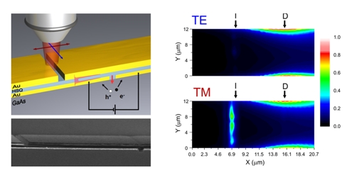 |
| Figure: Top left: schematic overview of the device, showing focused illumination of a slit in the waveguide using polarized light. This results in plasmon excitation of the waveguide for the red polarization and the generation of electron/hole pairs in the semiconductor. Bottom left: SEM picture of a typical device. Top/bottom right: Photocurrent scans for the �red� (bottom) and �blue� (top) polarization indicate a strong polarization dependence of the photoresponse � doi:10.1038/nphoton.2009.47 |
Abstract:
IMEC, Europe's leading independent nanoelectronics research institute, reports a method to integrate high-speed CMOS electronics and nanophotonic circuitry based on plasmonic effects. Metal-based nanophotonics (plasmonics) can squeeze light into nanoscale structures that are much smaller than conventional optic components. Plasmonic technology, today still in an experimental stage, has the potential to be used in future applications such as nanoscale optical interconnects for high performance computer chips, extremely sensitive (bio)molecular sensors, and highly efficient thin-film solar cells. IMEC's results are published in the May issue of Nature Photonics.
IMEC reports method to integrate plasmon-based nanophotonic circuitry with state-of-the-art ICs
Leuven, Belgium | Posted on May 4th, 2009The optical properties of nanostructured (noble) metals show great promise for use in nanophotonic applications. When such nanostructures are illuminated with visible to near-infrared light, the excitation of collective oscillations of conduction electrons - called surface plasmons - generates strong optical resonances. Moreover, surface plasmons are capable of capturing, guiding, and focusing electromagnetic energy in deep-subwavelength length-scales, i.e. smaller than the diffraction limit of the light. This is unlike conventional dielectric optical waveguides, which are limited by the wavelength of the light, and which therefore cannot be scaled down to tens of nanometers, which is the dimension of the components on today's nanoelectronic ICs.
Nanoscale plasmonic circuits would allow massive parallel routing of optical information on ICs. But eventually that high-bandwidth optical information has to be converted to electrical signals. To make such ICs that combine high-speed CMOS electronics and plasmonic circuitry, efficient and fast interfacing components are needed that couple the signals from plasmon waveguides to electrical devices.
As an important stepping stone to such components, IMEC has now demonstrated integrated electrical detection of highly confined short-wavelength surface plasmon polaritons in metal-dielectric-metal plasmon waveguides. The detection was done by embedding a photodetector in a metal plasmon waveguide. Because the waveguide and the photodetector have the same nanoscale dimensions, there is an efficient coupling of the surface plasmons into the photodetector and an ultrafast response. IMEC has set up a number of experiments that unambiguously demonstrate this electrical detection. The strong measured polarization dependence, the experimentally obtained influence of the waveguide length and the measured spectral response are all in line with theoretical expectations, obtained from finite element and finite-difference-time-domain calculations. These results pave the way for the integration of nanoscale plasmonic circuitry and high-speed electronics.
####
About IMEC
IMEC is a world-leading independent research center in nanoelectronics and nanotechnology. IMEC vzw is headquartered in Leuven, Belgium, has a sister company in the Netherlands, IMEC-NL, offices in the US, China and Taiwan, and representatives in Japan. Its staff of more than 1650 people includes about 550 industrial residents and guest researchers. In 2008, its revenue (P&L) was EUR 270.16 million.
IMEC�s More Moore research aims at semiconductor scaling towards 22nm and beyond. With its More than Moore research, IMEC looks into technologies for nomadic embedded systems, wireless autonomous transducer solutions, biomedical electronics, photovoltaics, organic electronics and GaN power electronics.
IMEC�s research bridges the gap between fundamental research at universities and technology development in industry. Its unique balance of processing and system know-how, intellectual property portfolio, state-of-the-art infrastructure and its strong network worldwide position IMEC as a key partner for shaping technologies for future systems.
For more information, please click here
Contacts:
Katrien Marent
Director of External Communications
T: +32 16 28 18 80
Copyright © IMEC
If you have a comment, please Contact us.Issuers of news releases, not 7th Wave, Inc. or Nanotechnology Now, are solely responsible for the accuracy of the content.
Bookmark:


| Related News Press |
News and information
![]() Quantum computer improves AI predictions April 17th, 2026
Quantum computer improves AI predictions April 17th, 2026
![]() Flexible sensor gains sensitivity under pressure April 17th, 2026
Flexible sensor gains sensitivity under pressure April 17th, 2026
![]() A reusable chip for particulate matter sensing April 17th, 2026
A reusable chip for particulate matter sensing April 17th, 2026
![]() Detecting vibrational quantum beating in the predissociation dynamics of SF6 using time-resolved photoelectron spectroscopy April 17th, 2026
Detecting vibrational quantum beating in the predissociation dynamics of SF6 using time-resolved photoelectron spectroscopy April 17th, 2026
Chip Technology
![]() A reusable chip for particulate matter sensing April 17th, 2026
A reusable chip for particulate matter sensing April 17th, 2026
![]() Metasurfaces smooth light to boost magnetic sensing precision January 30th, 2026
Metasurfaces smooth light to boost magnetic sensing precision January 30th, 2026
Nanoelectronics
![]() Lab to industry: InSe wafer-scale breakthrough for future electronics August 8th, 2025
Lab to industry: InSe wafer-scale breakthrough for future electronics August 8th, 2025
![]() Interdisciplinary: Rice team tackles the future of semiconductors Multiferroics could be the key to ultralow-energy computing October 6th, 2023
Interdisciplinary: Rice team tackles the future of semiconductors Multiferroics could be the key to ultralow-energy computing October 6th, 2023
![]() Key element for a scalable quantum computer: Physicists from Forschungszentrum J�lich and RWTH Aachen University demonstrate electron transport on a quantum chip September 23rd, 2022
Key element for a scalable quantum computer: Physicists from Forschungszentrum J�lich and RWTH Aachen University demonstrate electron transport on a quantum chip September 23rd, 2022
![]() Reduced power consumption in semiconductor devices September 23rd, 2022
Reduced power consumption in semiconductor devices September 23rd, 2022
Announcements
![]() A fundamentally new therapeutic approach to cystic fibrosis: Nanobody repairs cellular defect April 17th, 2026
A fundamentally new therapeutic approach to cystic fibrosis: Nanobody repairs cellular defect April 17th, 2026
![]() UC Irvine physicists discover method to reverse �quantum scrambling� : The work addresses the problem of information loss in quantum computing system April 17th, 2026
UC Irvine physicists discover method to reverse �quantum scrambling� : The work addresses the problem of information loss in quantum computing system April 17th, 2026
Photonics/Optics/Lasers
![]() Metasurfaces smooth light to boost magnetic sensing precision January 30th, 2026
Metasurfaces smooth light to boost magnetic sensing precision January 30th, 2026
![]() From sensors to smart systems: the rise of AI-driven photonic noses January 30th, 2026
From sensors to smart systems: the rise of AI-driven photonic noses January 30th, 2026
|
|
||
|
|
||
| The latest news from around the world, FREE | ||
|
|
||
|
|
||
| Premium Products | ||
|
|
||
|
Only the news you want to read!
Learn More |
||
|
|
||
|
Full-service, expert consulting
Learn More |
||
|
|
||