Home > Press > IMEC demonstrates 3D stacked integrated circuits
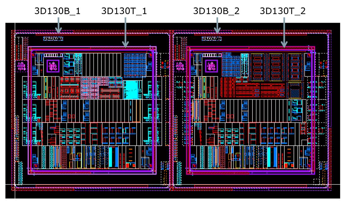 |
| Test-chip taped for assessing design rules and models for 3D-SIC technology. |
Abstract:
IMEC Annual Research Review Meeting - Leuven - Belgium
IMEC demonstrates 3D stacked integrated circuits
Leuven, Belgium | Posted on October 13th, 2008IMEC, Europe's leading independent nanoelectronics research institute today announced that it has made significant progress with its 3D-SIC (3D stacked IC) technology. IMEC recently demonstrated the first functional 3D integrated circuits obtained by die-to-die stacking using 5�m Cu through-silicon vias (TSV). It will now further develop 3D SIC chips on 200mm and 300mm wafers, integrating test circuits from partners participating in its 3D integration research program.
IMEC reported a first-time demonstration of 3D integrated circuits obtained by die-to-die stacking and using 5�m Cu through-silicon vias (TSV). The dies were realized on 200mm wafers in IMEC's reference 0.13μm CMOS process with an added Cu-TSVs process. For stacking, the top die was thinned down to 25μm and bonded to the landing die by Cu-Cu thermocompression. IMEC is upscaling the process for die-to-wafer bonding and is on track for migrating the process to its 300mm platform.
To evaluate the impact of the 3D SIC flow on the characteristics of the stacked layers, both the top and landing wafers contained CMOS circuits. Extensive tests confirmed that the performance of the circuits does not degrade with adding Cu TSVs and stacking. And to test the integrity and performance of the 3D stack, ring oscillators with varying configurations were made, distributed over the two chip layers and connected with the Cu TSVs. Tested after the TSV and stacking process, these circuits demonstrated the chips excellent integrity.
"With these tests, we have demonstrated that our technology allows designing and fabricating fully functional 3D SIC chips. We are now ready to accept reference test circuits from our industry partners," commented Eric Beyne, IMEC Scientific Director for 3D Technologies, "This will enable the industry to gain early insight and experience with 3D SIC design, using their own designs".
####
About IMEC
IMEC is a world-leading independent research center in nanoelectronics and nanotechnology. IMEC vzw is headquartered in Leuven, Belgium, has a sister company in the Netherlands, IMEC-NL, offices in the US, China and Taiwan, and representatives in Japan. Its staff of more than 1600 people includes more than 500 industrial residents and guest researchers. In 2007, its revenue (P&L) was EUR 244.5 million.
IMEC�s More Moore research aims at semiconductor scaling towards sub-32nm nodes. With its More than Moore research, IMEC looks into technologies for nomadic embedded systems, wireless autonomous transducer solutions, biomedical electronics, photovoltaics, organic electronics and GaN power electronics.
IMEC�s research bridges the gap between fundamental research at universities and technology development in industry. Its unique balance of processing and system know-how, intellectual property portfolio, state-of-the-art infrastructure and its strong network worldwide position IMEC as a key partner for shaping technologies for future systems.
For more information, please click here
Contacts:
Katrien Marent
Director of External Communications
T: +32 16 28 18 80
Mobile : +32 474 30 28 66
Copyright © IMEC
If you have a comment, please Contact us.Issuers of news releases, not 7th Wave, Inc. or Nanotechnology Now, are solely responsible for the accuracy of the content.
Bookmark:


| Related News Press |
News and information
![]() Quantum computer improves AI predictions April 17th, 2026
Quantum computer improves AI predictions April 17th, 2026
![]() Flexible sensor gains sensitivity under pressure April 17th, 2026
Flexible sensor gains sensitivity under pressure April 17th, 2026
![]() A reusable chip for particulate matter sensing April 17th, 2026
A reusable chip for particulate matter sensing April 17th, 2026
![]() Detecting vibrational quantum beating in the predissociation dynamics of SF6 using time-resolved photoelectron spectroscopy April 17th, 2026
Detecting vibrational quantum beating in the predissociation dynamics of SF6 using time-resolved photoelectron spectroscopy April 17th, 2026
Chip Technology
![]() A reusable chip for particulate matter sensing April 17th, 2026
A reusable chip for particulate matter sensing April 17th, 2026
![]() Metasurfaces smooth light to boost magnetic sensing precision January 30th, 2026
Metasurfaces smooth light to boost magnetic sensing precision January 30th, 2026
Nanoelectronics
![]() Lab to industry: InSe wafer-scale breakthrough for future electronics August 8th, 2025
Lab to industry: InSe wafer-scale breakthrough for future electronics August 8th, 2025
![]() Interdisciplinary: Rice team tackles the future of semiconductors Multiferroics could be the key to ultralow-energy computing October 6th, 2023
Interdisciplinary: Rice team tackles the future of semiconductors Multiferroics could be the key to ultralow-energy computing October 6th, 2023
![]() Key element for a scalable quantum computer: Physicists from Forschungszentrum J�lich and RWTH Aachen University demonstrate electron transport on a quantum chip September 23rd, 2022
Key element for a scalable quantum computer: Physicists from Forschungszentrum J�lich and RWTH Aachen University demonstrate electron transport on a quantum chip September 23rd, 2022
![]() Reduced power consumption in semiconductor devices September 23rd, 2022
Reduced power consumption in semiconductor devices September 23rd, 2022
Discoveries
![]() Quantum computer improves AI predictions April 17th, 2026
Quantum computer improves AI predictions April 17th, 2026
![]() Flexible sensor gains sensitivity under pressure April 17th, 2026
Flexible sensor gains sensitivity under pressure April 17th, 2026
![]() A reusable chip for particulate matter sensing April 17th, 2026
A reusable chip for particulate matter sensing April 17th, 2026
![]() Detecting vibrational quantum beating in the predissociation dynamics of SF6 using time-resolved photoelectron spectroscopy April 17th, 2026
Detecting vibrational quantum beating in the predissociation dynamics of SF6 using time-resolved photoelectron spectroscopy April 17th, 2026
Announcements
![]() A fundamentally new therapeutic approach to cystic fibrosis: Nanobody repairs cellular defect April 17th, 2026
A fundamentally new therapeutic approach to cystic fibrosis: Nanobody repairs cellular defect April 17th, 2026
![]() UC Irvine physicists discover method to reverse �quantum scrambling� : The work addresses the problem of information loss in quantum computing system April 17th, 2026
UC Irvine physicists discover method to reverse �quantum scrambling� : The work addresses the problem of information loss in quantum computing system April 17th, 2026
|
|
||
|
|
||
| The latest news from around the world, FREE | ||
|
|
||
|
|
||
| Premium Products | ||
|
|
||
|
Only the news you want to read!
Learn More |
||
|
|
||
|
Full-service, expert consulting
Learn More |
||
|
|
||