Home > Press > Bottoms Up: Better Organic Semiconductors for Printable Electronics
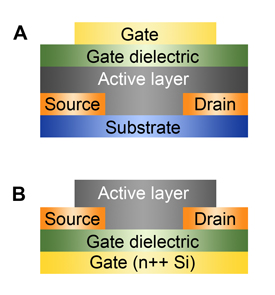 |
| Restacking organic semiconductors: An improved formulation for a polymer blend semiconductor causes key semiconducting molecules to migrate to the bottom of the active layer, allowing chip designers to replace top-gated structures (a) with more easily manufactured bottom-gate, bottom-contact devices (b).
Credit: Yoon, SNU/Talbott, NIST |
Abstract:
Researchers from the National Institute of Standards and Technology (NIST) and Seoul National University (SNU) have learned how to tweak a new class of polymer-based semiconductors to better control the location and alignment of the components of the blend. Their recent results—how to move the top to the bottom—could enable the design of practical, large-scale manufacturing techniques for a wide range of printable, flexible electronic displays and other devices.*
Bottoms Up: Better Organic Semiconductors for Printable Electronics
GAITHERSBURG, MD | Posted on September 3rd, 2008Organic semiconductors—novel carbon-based molecules that have similar electrical properties to more conventional semiconducting materials like silicon and germanium—are a hot research topic because practical, high-performance organic semiconductors would open up whole new categories of futuristic electronic devices. Think of tabloid-sized "digital paper" that you could fold up into your pocket or huge sheets of photovoltaic cells that are dirt cheap because they're manufactured by—basically—ink-jet printing.
The problem is performance. Small organic molecules have been developed with key electrical parameters close to the benchmark set by amorphous silicon semiconductors, but they are very difficult to deposit in a stable, uniform film—a key manufacturing requirement. Larger molecule polymer semiconductors, on the other hand, make excellent thin films but have at best limited semiconductor properties. A patent from British researchers in 2005 offered a promising compromise: blend the small semiconductor molecules in with the polymer. This works surprisingly well, but with an asterisk. Tests showed that actual devices, field effect transistors, made with the blend only worked well in a so-called "top-gated" structure. The critical active part of the film was on the top, and the switching part of the device (the "gate") had to be layered on top of that, a process difficult or impossible to do on a large scale without destroying the fragile film.
Working at NIST's Center for Neutron Research, the SNU/NIST research team used a neutron imaging technique that allowed them to observe, with nanometer resolution, how the distribution of small organic semiconductor molecules embedded in polymer films changed with depth—the films are less than 100 nanometers thick. In the thin films originally described by the patent, the bulk of the semiconductor molecules end up at the top of the film, as suspected. However, when the SNU/NIST research team substituted a polymer with significantly higher molecular mass, something interesting happened. The organic semiconductor small molecules distributed themselves evenly at the top and bottom of the film. Having an active region of the film on the bottom is key for large-scale manufacturing because it means the rest of the device—gate, source, drain—can be laid down first and the delicate film layer added last.
In addition, they report, the optimized blend of polymer and organic semiconductor actually has better performance characteristics than the organic semiconductor on its own.
* J. Kang, N. Shin, D.Y. Jang, V.M. Prabhu and D.Y. Yoon. Structure and properties of small molecule-polymer blend semiconductors for organic thin film transistors. Journal of the American Chemical Society, Published on the Web Aug. 23, 2008.
####
About NIST
Founded in 1901, NIST is a non-regulatory federal agency within the U.S. Department of Commerce. NIST's mission is to promote U.S. innovation and industrial competitiveness by advancing measurement science, standards, and technology in ways that enhance economic security and improve our quality of life.
For more information, please click here
Contacts:
Michael Baum
(301) 975-2763
Copyright © NIST
If you have a comment, please Contact us.Issuers of news releases, not 7th Wave, Inc. or Nanotechnology Now, are solely responsible for the accuracy of the content.
Bookmark:


| Related News Press |
News and information
![]() Quantum computer improves AI predictions April 17th, 2026
Quantum computer improves AI predictions April 17th, 2026
![]() Flexible sensor gains sensitivity under pressure April 17th, 2026
Flexible sensor gains sensitivity under pressure April 17th, 2026
![]() A reusable chip for particulate matter sensing April 17th, 2026
A reusable chip for particulate matter sensing April 17th, 2026
![]() Detecting vibrational quantum beating in the predissociation dynamics of SF6 using time-resolved photoelectron spectroscopy April 17th, 2026
Detecting vibrational quantum beating in the predissociation dynamics of SF6 using time-resolved photoelectron spectroscopy April 17th, 2026
Chip Technology
![]() A reusable chip for particulate matter sensing April 17th, 2026
A reusable chip for particulate matter sensing April 17th, 2026
![]() Metasurfaces smooth light to boost magnetic sensing precision January 30th, 2026
Metasurfaces smooth light to boost magnetic sensing precision January 30th, 2026
Discoveries
![]() Quantum computer improves AI predictions April 17th, 2026
Quantum computer improves AI predictions April 17th, 2026
![]() Flexible sensor gains sensitivity under pressure April 17th, 2026
Flexible sensor gains sensitivity under pressure April 17th, 2026
![]() A reusable chip for particulate matter sensing April 17th, 2026
A reusable chip for particulate matter sensing April 17th, 2026
![]() Detecting vibrational quantum beating in the predissociation dynamics of SF6 using time-resolved photoelectron spectroscopy April 17th, 2026
Detecting vibrational quantum beating in the predissociation dynamics of SF6 using time-resolved photoelectron spectroscopy April 17th, 2026
Announcements
![]() A fundamentally new therapeutic approach to cystic fibrosis: Nanobody repairs cellular defect April 17th, 2026
A fundamentally new therapeutic approach to cystic fibrosis: Nanobody repairs cellular defect April 17th, 2026
![]() UC Irvine physicists discover method to reverse ‘quantum scrambling’ : The work addresses the problem of information loss in quantum computing system April 17th, 2026
UC Irvine physicists discover method to reverse ‘quantum scrambling’ : The work addresses the problem of information loss in quantum computing system April 17th, 2026
Research partnerships
![]() Lab to industry: InSe wafer-scale breakthrough for future electronics August 8th, 2025
Lab to industry: InSe wafer-scale breakthrough for future electronics August 8th, 2025
![]() HKU physicists uncover hidden order in the quantum world through deconfined quantum critical points April 25th, 2025
HKU physicists uncover hidden order in the quantum world through deconfined quantum critical points April 25th, 2025
Printing/Lithography/Inkjet/Inks/Bio-printing/Dyes
![]() Presenting: Ultrasound-based printing of 3D materials—potentially inside the body December 8th, 2023
Presenting: Ultrasound-based printing of 3D materials—potentially inside the body December 8th, 2023
![]() Simple ballpoint pen can write custom LEDs August 11th, 2023
Simple ballpoint pen can write custom LEDs August 11th, 2023
![]() Disposable electronics on a simple sheet of paper October 7th, 2022
Disposable electronics on a simple sheet of paper October 7th, 2022
|
|
||
|
|
||
| The latest news from around the world, FREE | ||
|
|
||
|
|
||
| Premium Products | ||
|
|
||
|
Only the news you want to read!
Learn More |
||
|
|
||
|
Full-service, expert consulting
Learn More |
||
|
|
||