Home > Press > Destroying the superconductivity in a kagome metal: Electronic control of quantum transitions in candidate material for future low-energy electronics
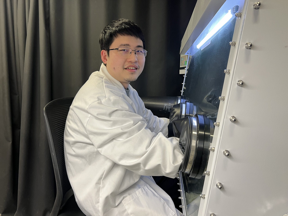 |
| Co-first author FLEET Research Fellow Dr Cheng Tan (RMIT) CREDIT FLEET |
Abstract:
Electrically controlled superconductor-to-“failed insulator” transition, and giant anomalous Hall effect in the kagome metal CsV3Sb5
Destroying the superconductivity in a kagome metal: Electronic control of quantum transitions in candidate material for future low-energy electronics
Melbourne, Australia | Posted on March 3rd, 2023A new RMIT-led international collaboration published in February has uncovered, for the first time, a distinct disorder-driven bosonic superconductor-insulator transition.
The discovery outlines a global picture of the giant anomalous Hall effect and reveals its correlation with the unconventional charge density wave in the AV3Sb5 kagome metal family, with potential applications in future ultra-low energy electronics.
Superconductors, which can transmit electricity without energy dissipation, hold great promise for the development of future low-energy electronics technologies, and are already applied in diverse fields such as hover trains and high-strength magnets (such as medical MRIs).
However, precisely how the superconductivity forms and works in many materials remains an unsolved issue and limits its applications.
Recently, a new kagome superconductor family AV₃Sb₅ has attracted intensive interest for their novel properties. ‘Kagome’ materials feature an unusual lattice named for a Japanese basket-weave pattern with corner-sharing triangles.
The AV₃Sb₅ materials (where A refers to caesium, rubidium, or potassium) provide ideal platforms for physics studies such as topology and strong correlations, but despite many recent investigations, the origin of the material’s giant anomalous Hall effect and superconductivity remain in debate.
The FLEET-led collaboration of researchers at RMIT University (Australia) and partner organisation the High Magnetic Field Laboratory (China) confirm for the first time the electric control of superconductivity and AHE in a van der Waals kagome metal CsV3Sb5.
Manipulating giant anomalous Hall effect via reversible proton intercalation
Possessing topological electron bands and geometrical frustration of vanadium lattices, the layered kagome metals AV3Sb5 have attracted great interests in condensed matter physics due to the many quantum phenomena that they support including:
unconventional, novel nematic order
chiral charge density order
giant anomalous Hall effect (AHE), and
the interplay between two-gap superconductivity and charge density wave (CDW) in AV3Sb5.
Moreover, the origin of giant AHE in AV3Sb5 and its correlation with chiral CDW remain elusive, in spite of several recently proposed mechanisms including the extrinsic skew scattering of Dirac quasiparticles with frustrated magnetic sublattice, the orbital currents of novel chiral charge order and the chiral flux phase in the CDW phase.
“Up to now, we had obtained many intriguing results with proton gate technique in vdW spintronic devices. Since this technique can effectively modulate the carrier density up to 1021 cm-3, we would like to apply it on AV3Sb5, which harbours a similar carrier density level.” says the new study’s first author, FLEET Research Fellow Dr Guolin Zheng (RMIT).
“The ability to tune the carrier density and the corresponding Fermi surfaces would play a vital role in understanding and manipulating these novel quantum states and would potentially realize some exotic quantum phase transitions.”
The team chose to test this theory on CsV3Sb5 which potentially has the largest spare atom space for proton intercalation. The devices were easily designed and fabricated based on the team’s rich experience in this field.
Their subsequent results with CsV3Sb5 depended strongly on material thickness.
“It was very difficult to effectively modulate the ‘thicker’ nanoflakes (more than 100 nm),” says co-first author, FLEET Research Fellow Dr Cheng Tan (RMIT).
“But when the thickness went down to around 40 nm, the injection of the proton became quite easy,” says Cheng. “We even found that the injection is highly reversible. Indeed, we have seldom met such a proton-friendly material!”
Interestingly, with the evolving proton intercalation, the carrier type (or the ‘sign’ of the Hall effect) could be modulated to either hole or electron type and the amplitude of the AHEs achieved were effectively tuned as well.
Further experimental and theoretical investigations indicate that this dramatic modulation of giant AHE originates from the Fermi level shift in the reconstructed band structures.
“The results of the gated AHE also revealed that the most possible origin of the AHE is skew scattering and this further improves our understanding on the kagome metal,” explains Guolin. “But we have not yet observed superconductor-insulator transition in 40 nm nanoflakes.”
“We must further try thinner CsV3Sb5 nanoflakes to explore this.”
Proton intercalation induced superconductor-to-‘failed insulator’ transition
The unique coexistence of electronic correlations and band topology in AV3Sb5 allows for investigating intriguing transitions of these correlated states, such as superconductor-insulator transition, a quantum phase transition usually tuned by disorders, magnetic fields and electric gating.
By decreasing the number of atomic layers, the team took further steps to explore the potential quantum phase transitions in CsV3Sb5.
“At first I directly tried some <10 nm ultrathin nanoflakes,” says Cheng. “I did observe that the critical temperatures of the superconductivity phase decreased with the increasing proton intercalation, but I could not definitively confirm that the superconductivity disappeared, as it might still exist at milliKelvin temperatures, where we cannot reach. Also, the devices were very fragile when I tried to further increase the proton intercalation.”
So Cheng changed the strategy and dealt with the 10~20nm thicker nanoflakes, as well as trying different electrode materials to seek a better electrical contact.
This strategy met with success. The team, surprisingly, observed that the critical temperature of the CDW phase decreased and the temperature-dependent resistance curves exhibit a clear superconductor-to-insulator transition under increasing proton injection.
“The proton intercalation introduced the disorder and suppressed both CDW and superconducting phase coherence,” says contributing-author A/Prof Lan Wang (also at RMIT). “And this gave rise to a superconductor-insulator transition associated with localized Cooper pairs and featuring a saturated sheet resistance reaching up to 106 Ω for temperature approaching zero, dubbed a ‘failed insulator’”.
“Our work uncovers a distinct disorder-driven bosonic superconductor-insulator transition, outlines a global picture of the giant AHE and reveals its correlation with the unconventional CDW in the AV3Sb5 family.”
“This significant and electrically-controlled superconductor-insulator transition and anomalous Hall effect in kagome metals should inspire more investigations of the relevant intriguing physics, with promise for energy-saving nanoelectronic devices.”
The study
“Electrically controlled superconductor-tofailed insulator transition and giant anomalous Hall effect in kagome metal CsV3Sb5 nanoflakes” was published in Nature Communications in February 2023. (DOI: 10.1038/s41467-023-36208-6)
As well as support from the Australian Research Council, support was also provided by Natural Science Foundation of China, National Key R&D Program of the MOST of China, the HFIPS Director’s Fund and the CASHIPS Director’s Fund. This work was also partially supported by Youth Innovation Promotion Association of CAS and the High Magnetic Field Laboratory (China).
Experimental research was performed at the RMIT Micro Nano Research Facility (MNRF) in the Victorian Node of the Australian National Fabrication Facility (ANFF) and the RMIT Microscopy and Microanalysis Facility (RMMF).
Superconductors are studied within FLEET enabling technology B — nano-device fabrication, an Australian Research Council Centre of Excellence. The Centre for Future Low-Energy Electronics Technologies (FLEET) brings together over a hundred Australian and international experts, with the shared mission to develop a new generation of ultra-low energy electronics. The impetus behind such work is the increasing challenge of energy used in computation, which uses 5–8% of global electricity and is doubling every decade.
More information
Contact Dr Guolin Zheng
Contact Dr Cheng Tan
Contact A/Prof Lan Wang (RMIT)
Watch Future solutions to computation energy use
Connect @FLEETCentre
** images first published in Nature Communications DOI 10.1038/s41467-023-36208-6
####
For more information, please click here
Contacts:
Errol Hunt
ARC Centre of Excellence in Future Low-Energy Electronics Technologies
Office: 042-313-9210
Copyright © ARC Centre of Excellence in Future Low-Energy Electronics Technologies
If you have a comment, please Contact us.Issuers of news releases, not 7th Wave, Inc. or Nanotechnology Now, are solely responsible for the accuracy of the content.
Bookmark:


| Related Links |
| Related News Press |
News and information
![]() Quantum computer improves AI predictions April 17th, 2026
Quantum computer improves AI predictions April 17th, 2026
![]() Flexible sensor gains sensitivity under pressure April 17th, 2026
Flexible sensor gains sensitivity under pressure April 17th, 2026
![]() A reusable chip for particulate matter sensing April 17th, 2026
A reusable chip for particulate matter sensing April 17th, 2026
![]() Detecting vibrational quantum beating in the predissociation dynamics of SF6 using time-resolved photoelectron spectroscopy April 17th, 2026
Detecting vibrational quantum beating in the predissociation dynamics of SF6 using time-resolved photoelectron spectroscopy April 17th, 2026
Quantum Physics
![]() Detecting vibrational quantum beating in the predissociation dynamics of SF6 using time-resolved photoelectron spectroscopy April 17th, 2026
Detecting vibrational quantum beating in the predissociation dynamics of SF6 using time-resolved photoelectron spectroscopy April 17th, 2026
![]() Beyond silicon: Electronics at the scale of a single molecule January 30th, 2026
Beyond silicon: Electronics at the scale of a single molecule January 30th, 2026
Superconductivity
Possible Futures
![]() A fundamentally new therapeutic approach to cystic fibrosis: Nanobody repairs cellular defect April 17th, 2026
A fundamentally new therapeutic approach to cystic fibrosis: Nanobody repairs cellular defect April 17th, 2026
![]() UC Irvine physicists discover method to reverse ‘quantum scrambling’ : The work addresses the problem of information loss in quantum computing system April 17th, 2026
UC Irvine physicists discover method to reverse ‘quantum scrambling’ : The work addresses the problem of information loss in quantum computing system April 17th, 2026
Chip Technology
![]() A reusable chip for particulate matter sensing April 17th, 2026
A reusable chip for particulate matter sensing April 17th, 2026
![]() Metasurfaces smooth light to boost magnetic sensing precision January 30th, 2026
Metasurfaces smooth light to boost magnetic sensing precision January 30th, 2026
Discoveries
![]() Quantum computer improves AI predictions April 17th, 2026
Quantum computer improves AI predictions April 17th, 2026
![]() Flexible sensor gains sensitivity under pressure April 17th, 2026
Flexible sensor gains sensitivity under pressure April 17th, 2026
![]() A reusable chip for particulate matter sensing April 17th, 2026
A reusable chip for particulate matter sensing April 17th, 2026
![]() Detecting vibrational quantum beating in the predissociation dynamics of SF6 using time-resolved photoelectron spectroscopy April 17th, 2026
Detecting vibrational quantum beating in the predissociation dynamics of SF6 using time-resolved photoelectron spectroscopy April 17th, 2026
Announcements
![]() A fundamentally new therapeutic approach to cystic fibrosis: Nanobody repairs cellular defect April 17th, 2026
A fundamentally new therapeutic approach to cystic fibrosis: Nanobody repairs cellular defect April 17th, 2026
![]() UC Irvine physicists discover method to reverse ‘quantum scrambling’ : The work addresses the problem of information loss in quantum computing system April 17th, 2026
UC Irvine physicists discover method to reverse ‘quantum scrambling’ : The work addresses the problem of information loss in quantum computing system April 17th, 2026
Interviews/Book Reviews/Essays/Reports/Podcasts/Journals/White papers/Posters
![]() A fundamentally new therapeutic approach to cystic fibrosis: Nanobody repairs cellular defect April 17th, 2026
A fundamentally new therapeutic approach to cystic fibrosis: Nanobody repairs cellular defect April 17th, 2026
![]() UC Irvine physicists discover method to reverse ‘quantum scrambling’ : The work addresses the problem of information loss in quantum computing system April 17th, 2026
UC Irvine physicists discover method to reverse ‘quantum scrambling’ : The work addresses the problem of information loss in quantum computing system April 17th, 2026
Research partnerships
![]() Lab to industry: InSe wafer-scale breakthrough for future electronics August 8th, 2025
Lab to industry: InSe wafer-scale breakthrough for future electronics August 8th, 2025
![]() HKU physicists uncover hidden order in the quantum world through deconfined quantum critical points April 25th, 2025
HKU physicists uncover hidden order in the quantum world through deconfined quantum critical points April 25th, 2025
Quantum nanoscience
![]() Beyond silicon: Electronics at the scale of a single molecule January 30th, 2026
Beyond silicon: Electronics at the scale of a single molecule January 30th, 2026
![]() MXene nanomaterials enter a new dimension Multilayer nanomaterial: MXene flakes created at Drexel University show new promise as 1D scrolls January 30th, 2026
MXene nanomaterials enter a new dimension Multilayer nanomaterial: MXene flakes created at Drexel University show new promise as 1D scrolls January 30th, 2026
![]() ICFO researchers overcome long-standing bottleneck in single photon detection with twisted 2D materials August 8th, 2025
ICFO researchers overcome long-standing bottleneck in single photon detection with twisted 2D materials August 8th, 2025
|
|
||
|
|
||
| The latest news from around the world, FREE | ||
|
|
||
|
|
||
| Premium Products | ||
|
|
||
|
Only the news you want to read!
Learn More |
||
|
|
||
|
Full-service, expert consulting
Learn More |
||
|
|
||