Home > Press > Novel nanowire fabrication technique paves way for next generation spintronics
 |
| CREDIT Tokyo Tech |
Abstract:
As our world modernizes faster than ever before, there is an ever-growing need for better and faster electronics and computers. Spintronics is a new system which uses the spin of an electron, in addition to the charge state, to encode data, making the entire system faster and more efficient. Ferromagnetic nanowires with high coercivity (resistance to changes in magnetization) are required to realize the potential of spintronics. Especially L10-ordered (a type of crystal structure) cobalt–platinum (CoPt) nanowires.
Novel nanowire fabrication technique paves way for next generation spintronics
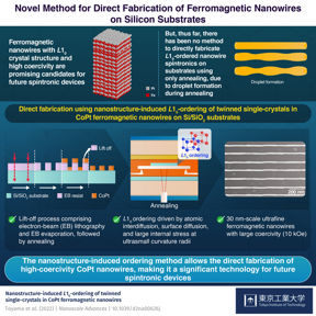
Tokyo, Japan | Posted on November 4th, 2022Conventional fabrication processes for L10-ordered nanowires involve heat treatment to improve the physical and chemical properties of the material, a process called annealing on the crystal substrate; the transfer of a pattern onto the substrate through lithography; and finally the chemical removal of layers through a process called etching. Eliminating the etching process by directly fabricating nanowires onto the silicon substrate would lead to a marked improvement in the fabrication of spintronic devices. However, when directly fabricated nanowires are subjected to annealing, they tend to transform into droplets as a result of the internal stresses in the wire.
Recently, a team of researchers led by Professor Yutaka Majima from the Tokyo Institute of Technology have found a solution to the problem. The team reported a new fabrication process to make L10-ordered CoPt nanowires on silicon/silicon dioxide (Si/SiO2) substrates. Talking about their research, published in Nanoscale Advances, Prof. Majima says, “Our nanostructure-induced ordering method allows the direct fabrication of ultrafine L10-ordered CoPt nanowires with the narrow widths of 30nm scale required for spintronics. This fabrication method could further be applied to other L10-ordered ferromagnetic materials such as iron–platinum and iron–palladium compounds.”
In this study, the researchers first coated a Si/SiO2 substrate with a material called a ‘resist’ and subjected it to electron beam lithography and evaporation to create a stencil for the nanowires. Then then deposited a multilayer of CoPt on the substrate. The deposited sampled were then ‘lifted-off’, leaving behind CoPt nanowires. These nanowires were then subjected to high temperature annealing. The researchers also examined the fabricated nanowires using several characterization techniques.
They found that the nanowires took on L10-ordering during the annealing process. This transformation was induced by atomic interdiffusion, surface diffusion, and extremely large internal stress at the ultrasmall 10 nm scale curvature radii of the nanowires. They also found that the nanowires exhibited a large coercivity of 10 kiloOersteds (kOe).
According to Prof. Majima, “The internal stresses on the nanostructure here induce the L10-ordering. This is a different mechanism than in previous studies. We are hopeful that this discovery will open up a new field of research called ‘nanostructure-induced materials science and engineering.’”
The wide applicability and convenience of the novel fabrication technique is sure to make a significant contribution to the field of spintronics research.
####
For more information, please click here
Contacts:
Reiko Hattori
Tokyo Institute of Technology
Office: +81-3-57343794
Copyright © Tokyo Institute of Technology
If you have a comment, please Contact us.Issuers of news releases, not 7th Wave, Inc. or Nanotechnology Now, are solely responsible for the accuracy of the content.
Bookmark:


| Related News Press |
News and information
![]() Researchers develop molecular qubits that communicate at telecom frequencies October 3rd, 2025
Researchers develop molecular qubits that communicate at telecom frequencies October 3rd, 2025
![]() Next-generation quantum communication October 3rd, 2025
Next-generation quantum communication October 3rd, 2025
![]() "Nanoreactor" cage uses visible light for catalytic and ultra-selective cross-cycloadditions October 3rd, 2025
"Nanoreactor" cage uses visible light for catalytic and ultra-selective cross-cycloadditions October 3rd, 2025
Physics
![]() Quantum computers simulate fundamental physics: shedding light on the building blocks of nature June 6th, 2025
Quantum computers simulate fundamental physics: shedding light on the building blocks of nature June 6th, 2025
![]() A 1960s idea inspires NBI researchers to study hitherto inaccessible quantum states June 6th, 2025
A 1960s idea inspires NBI researchers to study hitherto inaccessible quantum states June 6th, 2025
![]() Magnetism in new exotic material opens the way for robust quantum computers June 4th, 2025
Magnetism in new exotic material opens the way for robust quantum computers June 4th, 2025
Possible Futures
![]() Spinel-type sulfide semiconductors to operate the next-generation LEDs and solar cells For solar-cell absorbers and green-LED source October 3rd, 2025
Spinel-type sulfide semiconductors to operate the next-generation LEDs and solar cells For solar-cell absorbers and green-LED source October 3rd, 2025
Spintronics
![]() Quantum materials: Electron spin measured for the first time June 9th, 2023
Quantum materials: Electron spin measured for the first time June 9th, 2023
Quantum Computing
![]() Researchers develop molecular qubits that communicate at telecom frequencies October 3rd, 2025
Researchers develop molecular qubits that communicate at telecom frequencies October 3rd, 2025
![]() Researchers tackle the memory bottleneck stalling quantum computing October 3rd, 2025
Researchers tackle the memory bottleneck stalling quantum computing October 3rd, 2025
![]() Japan launches fully domestically produced quantum computer: Expo visitors to experience quantum computing firsthand August 8th, 2025
Japan launches fully domestically produced quantum computer: Expo visitors to experience quantum computing firsthand August 8th, 2025
Discoveries
![]() Researchers develop molecular qubits that communicate at telecom frequencies October 3rd, 2025
Researchers develop molecular qubits that communicate at telecom frequencies October 3rd, 2025
![]() Next-generation quantum communication October 3rd, 2025
Next-generation quantum communication October 3rd, 2025
![]() "Nanoreactor" cage uses visible light for catalytic and ultra-selective cross-cycloadditions October 3rd, 2025
"Nanoreactor" cage uses visible light for catalytic and ultra-selective cross-cycloadditions October 3rd, 2025
Announcements
![]() Rice membrane extracts lithium from brines with greater speed, less waste October 3rd, 2025
Rice membrane extracts lithium from brines with greater speed, less waste October 3rd, 2025
![]() Researchers develop molecular qubits that communicate at telecom frequencies October 3rd, 2025
Researchers develop molecular qubits that communicate at telecom frequencies October 3rd, 2025
![]() Next-generation quantum communication October 3rd, 2025
Next-generation quantum communication October 3rd, 2025
![]() "Nanoreactor" cage uses visible light for catalytic and ultra-selective cross-cycloadditions October 3rd, 2025
"Nanoreactor" cage uses visible light for catalytic and ultra-selective cross-cycloadditions October 3rd, 2025
Interviews/Book Reviews/Essays/Reports/Podcasts/Journals/White papers/Posters
![]() Spinel-type sulfide semiconductors to operate the next-generation LEDs and solar cells For solar-cell absorbers and green-LED source October 3rd, 2025
Spinel-type sulfide semiconductors to operate the next-generation LEDs and solar cells For solar-cell absorbers and green-LED source October 3rd, 2025
![]() Rice membrane extracts lithium from brines with greater speed, less waste October 3rd, 2025
Rice membrane extracts lithium from brines with greater speed, less waste October 3rd, 2025
|
|
||
|
|
||
| The latest news from around the world, FREE | ||
|
|
||
|
|
||
| Premium Products | ||
|
|
||
|
Only the news you want to read!
Learn More |
||
|
|
||
|
Full-service, expert consulting
Learn More |
||
|
|
||