Home > Press > On-Chip Photodetection: Two-dimensional material heterojunctions hetero-integration
 |
| CREDIT by Ruijuan Tian, Xuetao Gan, Chen Li, Xiaoqing Chen, Siqi Hu, Linpeng Gu, Dries Van Thourhout, Andres Castellanos-Gomez, Zhipei Sun, Jianlin Zhao |
Abstract:
Photonic integrated circuits (PICs) use photons as information carriers and are expected to solve the bottleneck problems of microelectronic chips in terms of speed, power consumption and integration density with their advantages of ultra-high transmission speed, low delay, and anti-electromagnetic crosstalk. It is of key significance to promoting breakthroughs in microelectronics technology, quantum information technology, and micro-sensing technology in the "post-Moore era".
On-Chip Photodetection: Two-dimensional material heterojunctions hetero-integration
Changchun, China | Posted on May 13th, 2022Currently, driven by the application of information technology, photonic integrated chips (PICs) have made great progress. For example, silicon PIC is compatible with the mature CMOS technology for low-cost and large-scale production; Silicon nitride PIC could tolerate moderately high optical power and large fabrication errors; Lithium niobate PIC could achieve perfect electro-optic modulations with low driven voltage and high linearity.
However, one of the handicaps in these PICs is the monolithic integration of waveguides and photodetectors with a single material. To support the light transmission in the waveguide, the PIC materials cannot absorb the optical signal, making it impossible to realize the integrated photodetector out of a single material. To solve this, hetero-integrations of absorptive bulk materials (such as Ge, III-V compound semiconductors, etc.) on PICs have been implemented. It though still present open challenges such as the high costs, complicated fabrication processes and material interface issues.
Recently, two-dimensional (2D) materials have emerged as an attractive photon-absorption material for chip-integrated photodetectors. 2D materials have no surface dangling bonds, which eliminates the lattice-mismatch constraints to hetero-integrate them with PICs. The family of 2D materials has a rich variety of electronic and optical properties, including semi-metallic graphene, insulating boron nitride, semiconducting transition metal dichalcogenides and black phosphorus. As a consequence, chip-integrated photodetectors operating at various spectral ranges could be constructed by choosing appropriate 2D materials.
In a new paper published in Light Science & Application, a research group, led by Professor Xuetao Gan from Key Laboratory of Light Field Manipulation and Information Acquisition, Ministry of Industry and Information Technology, and Shaanxi Key Laboratory of Optical Information Technology, School of Physical Science and Technology, Northwestern Polytechnical University, China have reported that integrating van der Waals PN heterojunctions of 2D materials on optical waveguides can provide a promising strategy to realize chip-integrated photodetectors with low dark current, high responsivity, and fast speed.
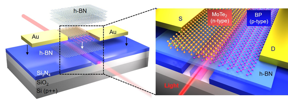
With the 2D layered structure and no dangling bonds, researchers can stack 2D materials with different properties in different orders by "stacking wood" to form van der Waals heterostructures with atomically flat interfaces. The "arbitrary combination" of van der Waals heterojunctions can not only give the advantages properties of a single material, but also generate novel properties, achieving a leap of 1+1>2, as shown in Figure 1. In this research, the researchers made full use of natural p-doped BP and n-doped MoTe2 for hetero-stacking, and successfully fabricated an efficient van der Waals PN heterojunction. Second, since there are no dangling bonds on the surface of 2D materials, compared with traditional semiconductors, 2D materials do not need to consider lattice mismatch when integrating with various photonic integration platforms. Finally, the preparation of source-drain electrodes can also be integrated on the photonic platform through the "stacking wood" technology and placed on both sides of the material, without the cumbersome processes such as photolithography. This also greatly simplifies the fabrication process of the device and reduces the fabrication cost of the device. This also greatly simplifies the fabrication process of the device, avoiding the contamination of the device interface in processes such as photolithography, which greatly improves the performance of the device.
####
For more information, please click here
Contacts:
Yaobiao Li
Light Publishing Center, Changchun Institute of Optics, Fine Mechanics And Physics, CAS
Office: 86-431-861-76851
Expert Contact
Xuetao Gan
Northwestern Polytechnical University, China
Copyright © Light Publishing Center, Changchun Institute of Optics, Fine Mechanics And Physics, CAS
If you have a comment, please Contact us.Issuers of news releases, not 7th Wave, Inc. or Nanotechnology Now, are solely responsible for the accuracy of the content.
Bookmark:


| Related Links |
| Related News Press |
News and information
![]() Quantum computer improves AI predictions April 17th, 2026
Quantum computer improves AI predictions April 17th, 2026
![]() Flexible sensor gains sensitivity under pressure April 17th, 2026
Flexible sensor gains sensitivity under pressure April 17th, 2026
![]() A reusable chip for particulate matter sensing April 17th, 2026
A reusable chip for particulate matter sensing April 17th, 2026
![]() Detecting vibrational quantum beating in the predissociation dynamics of SF6 using time-resolved photoelectron spectroscopy April 17th, 2026
Detecting vibrational quantum beating in the predissociation dynamics of SF6 using time-resolved photoelectron spectroscopy April 17th, 2026
Govt.-Legislation/Regulation/Funding/Policy
![]() Quantum computer improves AI predictions April 17th, 2026
Quantum computer improves AI predictions April 17th, 2026
![]() Metasurfaces smooth light to boost magnetic sensing precision January 30th, 2026
Metasurfaces smooth light to boost magnetic sensing precision January 30th, 2026
![]() New imaging approach transforms study of bacterial biofilms August 8th, 2025
New imaging approach transforms study of bacterial biofilms August 8th, 2025
Possible Futures
![]() A fundamentally new therapeutic approach to cystic fibrosis: Nanobody repairs cellular defect April 17th, 2026
A fundamentally new therapeutic approach to cystic fibrosis: Nanobody repairs cellular defect April 17th, 2026
![]() UC Irvine physicists discover method to reverse �quantum scrambling� : The work addresses the problem of information loss in quantum computing system April 17th, 2026
UC Irvine physicists discover method to reverse �quantum scrambling� : The work addresses the problem of information loss in quantum computing system April 17th, 2026
Chip Technology
![]() A reusable chip for particulate matter sensing April 17th, 2026
A reusable chip for particulate matter sensing April 17th, 2026
![]() Metasurfaces smooth light to boost magnetic sensing precision January 30th, 2026
Metasurfaces smooth light to boost magnetic sensing precision January 30th, 2026
Optical computing/Photonic computing
![]() ICFO researchers overcome long-standing bottleneck in single photon detection with twisted 2D materials August 8th, 2025
ICFO researchers overcome long-standing bottleneck in single photon detection with twisted 2D materials August 8th, 2025
![]() Programmable electron-induced color router array May 14th, 2025
Programmable electron-induced color router array May 14th, 2025
Discoveries
![]() Quantum computer improves AI predictions April 17th, 2026
Quantum computer improves AI predictions April 17th, 2026
![]() Flexible sensor gains sensitivity under pressure April 17th, 2026
Flexible sensor gains sensitivity under pressure April 17th, 2026
![]() A reusable chip for particulate matter sensing April 17th, 2026
A reusable chip for particulate matter sensing April 17th, 2026
![]() Detecting vibrational quantum beating in the predissociation dynamics of SF6 using time-resolved photoelectron spectroscopy April 17th, 2026
Detecting vibrational quantum beating in the predissociation dynamics of SF6 using time-resolved photoelectron spectroscopy April 17th, 2026
Announcements
![]() A fundamentally new therapeutic approach to cystic fibrosis: Nanobody repairs cellular defect April 17th, 2026
A fundamentally new therapeutic approach to cystic fibrosis: Nanobody repairs cellular defect April 17th, 2026
![]() UC Irvine physicists discover method to reverse �quantum scrambling� : The work addresses the problem of information loss in quantum computing system April 17th, 2026
UC Irvine physicists discover method to reverse �quantum scrambling� : The work addresses the problem of information loss in quantum computing system April 17th, 2026
Interviews/Book Reviews/Essays/Reports/Podcasts/Journals/White papers/Posters
![]() A fundamentally new therapeutic approach to cystic fibrosis: Nanobody repairs cellular defect April 17th, 2026
A fundamentally new therapeutic approach to cystic fibrosis: Nanobody repairs cellular defect April 17th, 2026
![]() UC Irvine physicists discover method to reverse �quantum scrambling� : The work addresses the problem of information loss in quantum computing system April 17th, 2026
UC Irvine physicists discover method to reverse �quantum scrambling� : The work addresses the problem of information loss in quantum computing system April 17th, 2026
Grants/Sponsored Research/Awards/Scholarships/Gifts/Contests/Honors/Records
![]() Quantum computer improves AI predictions April 17th, 2026
Quantum computer improves AI predictions April 17th, 2026
![]() Detecting vibrational quantum beating in the predissociation dynamics of SF6 using time-resolved photoelectron spectroscopy April 17th, 2026
Detecting vibrational quantum beating in the predissociation dynamics of SF6 using time-resolved photoelectron spectroscopy April 17th, 2026
![]() Metasurfaces smooth light to boost magnetic sensing precision January 30th, 2026
Metasurfaces smooth light to boost magnetic sensing precision January 30th, 2026
Photonics/Optics/Lasers
![]() Metasurfaces smooth light to boost magnetic sensing precision January 30th, 2026
Metasurfaces smooth light to boost magnetic sensing precision January 30th, 2026
![]() From sensors to smart systems: the rise of AI-driven photonic noses January 30th, 2026
From sensors to smart systems: the rise of AI-driven photonic noses January 30th, 2026
Printing/Lithography/Inkjet/Inks/Bio-printing/Dyes
![]() Presenting: Ultrasound-based printing of 3D materials�potentially inside the body December 8th, 2023
Presenting: Ultrasound-based printing of 3D materials�potentially inside the body December 8th, 2023
![]() Simple ballpoint pen can write custom LEDs August 11th, 2023
Simple ballpoint pen can write custom LEDs August 11th, 2023
![]() Disposable electronics on a simple sheet of paper October 7th, 2022
Disposable electronics on a simple sheet of paper October 7th, 2022
|
|
||
|
|
||
| The latest news from around the world, FREE | ||
|
|
||
|
|
||
| Premium Products | ||
|
|
||
|
Only the news you want to read!
Learn More |
||
|
|
||
|
Full-service, expert consulting
Learn More |
||
|
|
||