Home > Press > Monolayer transition metal dichalcogenide lens for high resolution imaging
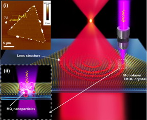 |
| Schematic of femtosecond laser fabrication of a monolayer TMDC lens. Inset: (i) AFM image of a monolayer TMDC single crystal, and (ii) Schematic of femtosecond laser-induced generation of MOx nanoparticles. CREDIT by Han Lin, Zai-Quan Xu, Guiyuan Cao, Yupeng Zhang, Jiadong Zhou, Ziyu Wang, Zhichen Wan, Zheng Liu, Kian Ping Loh, Cheng-Wei Qiu, Qiaoliang Bao, Baohua Jia |
Abstract:
Lenses are one of the most commonly used optical components in daily life, including eyeglasses, microscopic objectives, magnifying glass, and camera lenses. Conventional lenses are based on the principle of light refraction, using different materials, spherical surfaces and spatial positions to achieve the control of light. The fabrication of conventional lenses including the processes of material selection, cutting, rough grinding, fine grinding, polishing, and testing. In order to minimize the aberrations including the chromatic aberration, spherical aberration and astigmatisms, it is necessary to stack multiple layers of lenses to form compound lenses, leading to the complexity and cumbersomeness of current camera equipment.
Monolayer transition metal dichalcogenide lens for high resolution imaging
Changchun, China | Posted on August 14th, 2020Therefore, tremendous effort has been devoted into the development of ultrathin flat lenses. Unlike conventional lenses, flat lenses use nanostructures to modulate light. By controlling the optical properties and the spatial position of each nano-element, advanced functions, such as achromatic and aberration-free focusing, high spatial resolution and special focal intensity distributions can be achieved. However, when the material thickness is reduced to the subwavelength scale, the insufficient phase or amplitude modulation based on the intrinsic refractive index and absorption of the materials results in poor lens performance.
In a new paper published in Light Science & Application, a team of scientists, led by Prof. Baohua Jia at Centre for Translational Atomaterials, Swinburne University of Technology, Australia, Prof. Qiaoliang Bao formerly at Monash University, Prof. Chengwei Qiu at National University of Singapore and co-workers have developed an innovative method to fabricate high performance lenses in monolayer two dimensional transitional metal dichalcogenide (TMDC) material by using a femtosecond laser to pattern nanoparticles. The lens has a sub-wavelength resolution and a focusing efficiency of 31%, laying the foundation for ultimately thin optical devices for use in nano-optics and on-chip photonic applications.
Although lenses made from multilayer TMDCs have been demonstrated before, when their thickness is reduced to the sub-nanometer scale, their insufficient phase or amplitude modulation results in focusing efficiencies of less than 1%. The international team discovered that it is possible to generate nanoparticles by using a femtosecond laser beam to interact with the monolayer TMDC material, which is significantly different from the process produced by a continuous wave laser. When the laser pulse is so short that the entire material remains cold after laser process, the nanoparticles can firmly attach to the substrate. The nanoparticles show very strong scattering to modulate the amplitude of light. Therefore, the lens made from the nanoparticles can provide subwavelength resolution and high efficiency, which allows the team to demonstrate diffraction-limited imaging by using the lenses.
Monolayer is the thinnest form of a material, which is the ultimate physical thickness limit. By using the monolayer for the lens fabrication, the process demonstrated in this study consumed the least material meeting the theoretical limitation. More importantly, the femtosecond laser fabrication technique is a one-step simple process, without the requirements of high vacuum or special environment, thus it provides the simplest way to fabricate an ultrathin flat lens. As a result, the lens can be easily integrated into any photonic or microfluidic devices for broad applications.
"We have used the thinnest material in the world to fabricate a flat lens, and prove that the good performance of the ultrathin lens can lead to high resolution imaging. It shows enormous potential in different applications, such as eyeglasses, microscopy lenses, telescopes and camera lenses. It is foreseeable that by using this technique, the weight and size of camera lenses can be significantly reduced in the near future." Said Dr Han Lin, the first author from the Centre for Translational Atomaterials, Swinburne University of Technology.
"We are excited to see unique outcome from femtosecond laser processing 2D materials. It opens up new possibility to fabrication photonic devices using scalable method." Added by Prof. Baohua Jia, Director of Centre for Translational Atomaterials.
"We can integrate the monolayer 2D material lens onto desired devices by simply attaching the material then using a femtosecond laser to perform fabrication. The entire process is simple, and the method is flexible and low cost. Thus, we also see the great application potential of the method." Commented by Prof. Qiaoliang Bao formerly at Monash University.
"We design our lens in such a way that image can be found at different focal planes, with different magnifications. This mechanism can be readily used to develop an optical zoom lens that is required in all cellphone cameras. Currently, lenses with different focal lengths are used to achieve different zoom function. However, our lenses can achieve different zoom rates simply with one design." Prof. Chengwei Qiu from National University of Singapore forecasts.
####
For more information, please click here
Contacts:
Baohua Jia
Copyright © Changchun Institute of Optics, Fine Mechanics and Physics, Chinese Academy of Sciences
If you have a comment, please Contact us.Issuers of news releases, not 7th Wave, Inc. or Nanotechnology Now, are solely responsible for the accuracy of the content.
Bookmark:


| Related Links |
| Related News Press |
News and information
![]() Quantum computer improves AI predictions April 17th, 2026
Quantum computer improves AI predictions April 17th, 2026
![]() Flexible sensor gains sensitivity under pressure April 17th, 2026
Flexible sensor gains sensitivity under pressure April 17th, 2026
![]() A reusable chip for particulate matter sensing April 17th, 2026
A reusable chip for particulate matter sensing April 17th, 2026
![]() Detecting vibrational quantum beating in the predissociation dynamics of SF6 using time-resolved photoelectron spectroscopy April 17th, 2026
Detecting vibrational quantum beating in the predissociation dynamics of SF6 using time-resolved photoelectron spectroscopy April 17th, 2026
2 Dimensional Materials
![]() Flexible sensor gains sensitivity under pressure April 17th, 2026
Flexible sensor gains sensitivity under pressure April 17th, 2026
Govt.-Legislation/Regulation/Funding/Policy
![]() Quantum computer improves AI predictions April 17th, 2026
Quantum computer improves AI predictions April 17th, 2026
![]() Metasurfaces smooth light to boost magnetic sensing precision January 30th, 2026
Metasurfaces smooth light to boost magnetic sensing precision January 30th, 2026
![]() New imaging approach transforms study of bacterial biofilms August 8th, 2025
New imaging approach transforms study of bacterial biofilms August 8th, 2025
Possible Futures
![]() A fundamentally new therapeutic approach to cystic fibrosis: Nanobody repairs cellular defect April 17th, 2026
A fundamentally new therapeutic approach to cystic fibrosis: Nanobody repairs cellular defect April 17th, 2026
![]() UC Irvine physicists discover method to reverse �quantum scrambling� : The work addresses the problem of information loss in quantum computing system April 17th, 2026
UC Irvine physicists discover method to reverse �quantum scrambling� : The work addresses the problem of information loss in quantum computing system April 17th, 2026
Discoveries
![]() Quantum computer improves AI predictions April 17th, 2026
Quantum computer improves AI predictions April 17th, 2026
![]() Flexible sensor gains sensitivity under pressure April 17th, 2026
Flexible sensor gains sensitivity under pressure April 17th, 2026
![]() A reusable chip for particulate matter sensing April 17th, 2026
A reusable chip for particulate matter sensing April 17th, 2026
![]() Detecting vibrational quantum beating in the predissociation dynamics of SF6 using time-resolved photoelectron spectroscopy April 17th, 2026
Detecting vibrational quantum beating in the predissociation dynamics of SF6 using time-resolved photoelectron spectroscopy April 17th, 2026
Announcements
![]() A fundamentally new therapeutic approach to cystic fibrosis: Nanobody repairs cellular defect April 17th, 2026
A fundamentally new therapeutic approach to cystic fibrosis: Nanobody repairs cellular defect April 17th, 2026
![]() UC Irvine physicists discover method to reverse �quantum scrambling� : The work addresses the problem of information loss in quantum computing system April 17th, 2026
UC Irvine physicists discover method to reverse �quantum scrambling� : The work addresses the problem of information loss in quantum computing system April 17th, 2026
Interviews/Book Reviews/Essays/Reports/Podcasts/Journals/White papers/Posters
![]() A fundamentally new therapeutic approach to cystic fibrosis: Nanobody repairs cellular defect April 17th, 2026
A fundamentally new therapeutic approach to cystic fibrosis: Nanobody repairs cellular defect April 17th, 2026
![]() UC Irvine physicists discover method to reverse �quantum scrambling� : The work addresses the problem of information loss in quantum computing system April 17th, 2026
UC Irvine physicists discover method to reverse �quantum scrambling� : The work addresses the problem of information loss in quantum computing system April 17th, 2026
Grants/Sponsored Research/Awards/Scholarships/Gifts/Contests/Honors/Records
![]() Quantum computer improves AI predictions April 17th, 2026
Quantum computer improves AI predictions April 17th, 2026
![]() Detecting vibrational quantum beating in the predissociation dynamics of SF6 using time-resolved photoelectron spectroscopy April 17th, 2026
Detecting vibrational quantum beating in the predissociation dynamics of SF6 using time-resolved photoelectron spectroscopy April 17th, 2026
![]() Metasurfaces smooth light to boost magnetic sensing precision January 30th, 2026
Metasurfaces smooth light to boost magnetic sensing precision January 30th, 2026
Photonics/Optics/Lasers
![]() Metasurfaces smooth light to boost magnetic sensing precision January 30th, 2026
Metasurfaces smooth light to boost magnetic sensing precision January 30th, 2026
![]() From sensors to smart systems: the rise of AI-driven photonic noses January 30th, 2026
From sensors to smart systems: the rise of AI-driven photonic noses January 30th, 2026
Research partnerships
![]() Lab to industry: InSe wafer-scale breakthrough for future electronics August 8th, 2025
Lab to industry: InSe wafer-scale breakthrough for future electronics August 8th, 2025
![]() HKU physicists uncover hidden order in the quantum world through deconfined quantum critical points April 25th, 2025
HKU physicists uncover hidden order in the quantum world through deconfined quantum critical points April 25th, 2025
|
|
||
|
|
||
| The latest news from around the world, FREE | ||
|
|
||
|
|
||
| Premium Products | ||
|
|
||
|
Only the news you want to read!
Learn More |
||
|
|
||
|
Full-service, expert consulting
Learn More |
||
|
|
||