Home > Press > Light can 'heal' defects in new solar cell materials: Defects in some new electronic materials can be removed by making ions move under illumination
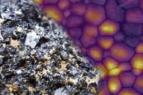 |
| A sample of the mineral perovskite is shown in the foreground, while behind it is an image the researchers used to prove the effects of intense light on a thin film of perovskite. Fluorescence imaging shows that areas that received more light became more purified, as revealed by brighter fluorescence from those regions.
Image: MIT News. Fluorescence image courtesy of the researchers. |
Abstract:
A family of compounds known as perovskites, which can be made into thin films with many promising electronic and optical properties, has been a hot research topic in recent years. But although these materials could potentially be highly useful in applications such as solar cells, some limitations still hamper their efficiency and consistency.
Light can 'heal' defects in new solar cell materials: Defects in some new electronic materials can be removed by making ions move under illumination
Cambridge, MA | Posted on May 24th, 2016Now, a team of researchers at MIT and elsewhere say they have made significant inroads toward understanding a process for improving perovskites' performance, by modifying the material using intense light. The new findings are being reported in the journal Nature Communications, in a paper by Samuel Stranks, a researcher at MIT; Vladimir Bulovic, the Fariborz Maseeh (1990) Professor of Emerging Technology and associate dean for innovation; and eight colleagues at other institutions in the U.S. and the U.K. The work is part of a major research effort on perovskite materials being led by Stranks, within MIT's Organic and Nanostructured Electronics Laboratory.
Tiny defects in perovskite's crystalline structure can hamper the conversion of light into electricity in a solar cell, but "what we're finding is that there are some defects that can be healed under light," says Stranks, who is a Marie Curie Fellow jointly at MIT and Cambridge University in the U.K. The tiny defects, called traps, can cause electrons to recombine with atoms before the electrons can reach a place in the crystal where their motion can be harnessed.
Under intense illumination, the researchers found that iodide ions -- atoms stripped of an electron so they carry an electric charge -- migrated away from the illuminated region, and in the process apparently swept away most of the defects in that region along with them.
"This is the first time this has been shown," Stranks says, "where just under illumination, where no [electric or magnetic] field has been applied, we see this ion migration that helps to clean the film. It reduces the defect density." While the effect had been observed before, this work is the first to show that the improvement was caused by the ions moving as a result of the illumination.
This work is focused on particular types of the material, known as organic-inorganic metal halide perovskites, which are considered promising for applications including solar cells, light-emitting diodes (LEDs), lasers, and light detectors. They excel in a property called the photoluminescence quantum efficiency, which is key to maximizing the efficiency of solar cells. But in practice, the performance of different batches of these materials, or even different spots on the same film, has been highly variable and unpredictable. The new work was aimed at figuring out what caused these discrepancies and how to reduce or eliminate them.
Stranks explains that "the ultimate aim is to make defect-free films," and the resulting improvements in efficiency could also be useful for applications in light emission as well as light capture.
Previous work reducing defects in thin-film perovskite materials has focused on electrical or chemical treatments, but "we find we can do the same with light," Stranks says. One advantage of that is that the same technique used to improve the material's properties can at the same time be used as a sensitive probe to observe and better understand the behavior of these promising materials.
Another advantage of this light-based processing is it doesn't require anything to come in physical contact with the film being treated -- for example, there is no need to attach electrical contacts or to bathe the material in a chemical solution. Instead, the treatment can simply be applied by turning on the source of illumination. The process, which they call photo-induced cleaning, could be "a way forward" for the development of useful perovskite-based devices, Stranks says.
The effects of the illumination tend to diminish over time, Stranks says, so "the challenge now is to maintain the effect" long enough to make it practical. Some forms of perovskites are already "looking to be commercialized by next year," he says, and this research "raises questions that need to be addressed, but it also shows there are ways to address" the phenomena that have been limiting this material's performance.
###
In addition to Stranks and Bulovic, the team included Anna Osherov of MIT, Dane deQuilettes, Daniel Graham, and David Ginger of the University of Washington, and Wei Zhang, Victor Burlakov, Tomas Leitjens, and Henry Snaith of Oxford University in the U.K. The work was supported by the European Union Seventh Framework Programme, the U.S. National Science Foundation, the Center for Excitonics, an Energy Frontier Research Center at MIT funded by the U.S. Department of Energy, and the National Institutes of Health.
####
For more information, please click here
Contacts:
Karl-Lydie Jean-Baptiste
617-253-1682
Copyright © Massachusetts Institute of Technology
If you have a comment, please Contact us.Issuers of news releases, not 7th Wave, Inc. or Nanotechnology Now, are solely responsible for the accuracy of the content.
Bookmark:


| Related Links |
![]() Paper: �Photo-induced halide redistribution in organic-inorganic perovskite films.�:
Paper: �Photo-induced halide redistribution in organic-inorganic perovskite films.�:
| Related News Press |
News and information
![]() Quantum computer improves AI predictions April 17th, 2026
Quantum computer improves AI predictions April 17th, 2026
![]() Flexible sensor gains sensitivity under pressure April 17th, 2026
Flexible sensor gains sensitivity under pressure April 17th, 2026
![]() A reusable chip for particulate matter sensing April 17th, 2026
A reusable chip for particulate matter sensing April 17th, 2026
![]() Detecting vibrational quantum beating in the predissociation dynamics of SF6 using time-resolved photoelectron spectroscopy April 17th, 2026
Detecting vibrational quantum beating in the predissociation dynamics of SF6 using time-resolved photoelectron spectroscopy April 17th, 2026
Imaging
![]() Simple algorithm paired with standard imaging tool could predict failure in lithium metal batteries August 8th, 2025
Simple algorithm paired with standard imaging tool could predict failure in lithium metal batteries August 8th, 2025
![]() First real-time observation of two-dimensional melting process: Researchers at Mainz University unveil new insights into magnetic vortex structures August 8th, 2025
First real-time observation of two-dimensional melting process: Researchers at Mainz University unveil new insights into magnetic vortex structures August 8th, 2025
Thin films
![]() Tiny nanosheets, big leap: A new sensor detects ethanol at ultra-low levels January 30th, 2026
Tiny nanosheets, big leap: A new sensor detects ethanol at ultra-low levels January 30th, 2026
Govt.-Legislation/Regulation/Funding/Policy
![]() Quantum computer improves AI predictions April 17th, 2026
Quantum computer improves AI predictions April 17th, 2026
![]() Metasurfaces smooth light to boost magnetic sensing precision January 30th, 2026
Metasurfaces smooth light to boost magnetic sensing precision January 30th, 2026
![]() New imaging approach transforms study of bacterial biofilms August 8th, 2025
New imaging approach transforms study of bacterial biofilms August 8th, 2025
Possible Futures
![]() A fundamentally new therapeutic approach to cystic fibrosis: Nanobody repairs cellular defect April 17th, 2026
A fundamentally new therapeutic approach to cystic fibrosis: Nanobody repairs cellular defect April 17th, 2026
![]() UC Irvine physicists discover method to reverse �quantum scrambling� : The work addresses the problem of information loss in quantum computing system April 17th, 2026
UC Irvine physicists discover method to reverse �quantum scrambling� : The work addresses the problem of information loss in quantum computing system April 17th, 2026
Discoveries
![]() Quantum computer improves AI predictions April 17th, 2026
Quantum computer improves AI predictions April 17th, 2026
![]() Flexible sensor gains sensitivity under pressure April 17th, 2026
Flexible sensor gains sensitivity under pressure April 17th, 2026
![]() A reusable chip for particulate matter sensing April 17th, 2026
A reusable chip for particulate matter sensing April 17th, 2026
![]() Detecting vibrational quantum beating in the predissociation dynamics of SF6 using time-resolved photoelectron spectroscopy April 17th, 2026
Detecting vibrational quantum beating in the predissociation dynamics of SF6 using time-resolved photoelectron spectroscopy April 17th, 2026
Materials/Metamaterials/Magnetoresistance
![]() First real-time observation of two-dimensional melting process: Researchers at Mainz University unveil new insights into magnetic vortex structures August 8th, 2025
First real-time observation of two-dimensional melting process: Researchers at Mainz University unveil new insights into magnetic vortex structures August 8th, 2025
![]() Researchers unveil a groundbreaking clay-based solution to capture carbon dioxide and combat climate change June 6th, 2025
Researchers unveil a groundbreaking clay-based solution to capture carbon dioxide and combat climate change June 6th, 2025
![]() A 1960s idea inspires NBI researchers to study hitherto inaccessible quantum states June 6th, 2025
A 1960s idea inspires NBI researchers to study hitherto inaccessible quantum states June 6th, 2025
![]() Institute for Nanoscience hosts annual proposal planning meeting May 16th, 2025
Institute for Nanoscience hosts annual proposal planning meeting May 16th, 2025
Announcements
![]() A fundamentally new therapeutic approach to cystic fibrosis: Nanobody repairs cellular defect April 17th, 2026
A fundamentally new therapeutic approach to cystic fibrosis: Nanobody repairs cellular defect April 17th, 2026
![]() UC Irvine physicists discover method to reverse �quantum scrambling� : The work addresses the problem of information loss in quantum computing system April 17th, 2026
UC Irvine physicists discover method to reverse �quantum scrambling� : The work addresses the problem of information loss in quantum computing system April 17th, 2026
Interviews/Book Reviews/Essays/Reports/Podcasts/Journals/White papers/Posters
![]() A fundamentally new therapeutic approach to cystic fibrosis: Nanobody repairs cellular defect April 17th, 2026
A fundamentally new therapeutic approach to cystic fibrosis: Nanobody repairs cellular defect April 17th, 2026
![]() UC Irvine physicists discover method to reverse �quantum scrambling� : The work addresses the problem of information loss in quantum computing system April 17th, 2026
UC Irvine physicists discover method to reverse �quantum scrambling� : The work addresses the problem of information loss in quantum computing system April 17th, 2026
Tools
![]() Metasurfaces smooth light to boost magnetic sensing precision January 30th, 2026
Metasurfaces smooth light to boost magnetic sensing precision January 30th, 2026
![]() From sensors to smart systems: the rise of AI-driven photonic noses January 30th, 2026
From sensors to smart systems: the rise of AI-driven photonic noses January 30th, 2026
![]() Japan launches fully domestically produced quantum computer: Expo visitors to experience quantum computing firsthand August 8th, 2025
Japan launches fully domestically produced quantum computer: Expo visitors to experience quantum computing firsthand August 8th, 2025
Energy
![]() Sensors innovations for smart lithium-based batteries: advancements, opportunities, and potential challenges August 8th, 2025
Sensors innovations for smart lithium-based batteries: advancements, opportunities, and potential challenges August 8th, 2025
![]() Simple algorithm paired with standard imaging tool could predict failure in lithium metal batteries August 8th, 2025
Simple algorithm paired with standard imaging tool could predict failure in lithium metal batteries August 8th, 2025
Grants/Sponsored Research/Awards/Scholarships/Gifts/Contests/Honors/Records
![]() Quantum computer improves AI predictions April 17th, 2026
Quantum computer improves AI predictions April 17th, 2026
![]() Detecting vibrational quantum beating in the predissociation dynamics of SF6 using time-resolved photoelectron spectroscopy April 17th, 2026
Detecting vibrational quantum beating in the predissociation dynamics of SF6 using time-resolved photoelectron spectroscopy April 17th, 2026
![]() Metasurfaces smooth light to boost magnetic sensing precision January 30th, 2026
Metasurfaces smooth light to boost magnetic sensing precision January 30th, 2026
Research partnerships
![]() Lab to industry: InSe wafer-scale breakthrough for future electronics August 8th, 2025
Lab to industry: InSe wafer-scale breakthrough for future electronics August 8th, 2025
![]() HKU physicists uncover hidden order in the quantum world through deconfined quantum critical points April 25th, 2025
HKU physicists uncover hidden order in the quantum world through deconfined quantum critical points April 25th, 2025
Solar/Photovoltaic
![]() Spinel-type sulfide semiconductors to operate the next-generation LEDs and solar cells For solar-cell absorbers and green-LED source October 3rd, 2025
Spinel-type sulfide semiconductors to operate the next-generation LEDs and solar cells For solar-cell absorbers and green-LED source October 3rd, 2025
![]() KAIST researchers introduce new and improved, next-generation perovskite solar cell November 8th, 2024
KAIST researchers introduce new and improved, next-generation perovskite solar cell November 8th, 2024
![]() Groundbreaking precision in single-molecule optoelectronics August 16th, 2024
Groundbreaking precision in single-molecule optoelectronics August 16th, 2024
![]() Development of zinc oxide nanopagoda array photoelectrode: photoelectrochemical water-splitting hydrogen production January 12th, 2024
Development of zinc oxide nanopagoda array photoelectrode: photoelectrochemical water-splitting hydrogen production January 12th, 2024
|
|
||
|
|
||
| The latest news from around the world, FREE | ||
|
|
||
|
|
||
| Premium Products | ||
|
|
||
|
Only the news you want to read!
Learn More |
||
|
|
||
|
Full-service, expert consulting
Learn More |
||
|
|
||