Home > Press > NbSe2, a true 2-D superconductor
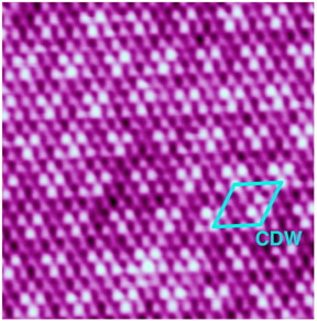 |
| Atomically resolved STM image of the NbSe2 surface showing CDW modulation. CREDIT: CIC nanoGUNE |
Abstract:
Very few 2D superconductors exist in nature, and single-layer NbSe2 is the first among them that remains a superconductor in its isolated, 2D form without the need of a special substrate. Furthermore, CDW order - spatial modulation of both the electron density and the atomic lattice (see figure below) - has been revealed to be a genuine 2D electronic phenomenon in NbSe2. This work has been recently reported in Nature Physics.
NbSe2, a true 2-D superconductor
Usurbil, Spain | Posted on November 5th, 2015Many-body interactions in solids are at the core of stunning collective electronic phenomena such as CDW order and superconductivity, which are found to exist in some TMD metals in their 3D bulk form. In reduced dimensions, materials usually exhibit remarkable differences in their properties with respect to their 3D bulk counterparts due to quantum confinement effects. In bulk NbSe2 a CDW sets in at TCDW = 33 K and superconductivity sets in at Tc = 7.2 K. Below 7.2 K these electronic states coexist but their microscopic formation mechanisms in bulk remain controversial after nearly four decades of intense research. Furthermore, the fate of its CDW and superconducting phases in the ultimate single-layer limit has also remained mysterious until now. Writing in Nature Physics, the team has characterized the electronic structure of a single layer of NbSe2 directly grown on graphene, which experimentally confirms that NbSe2 undergoes a reduction in the number of electronic bands involved in its collective phases (from three bands in bulk NbSe2 to just one for single-layer NbSe2). Despite significant changes in NbSe2 electronic structure upon dimensional reduction, the authors show that - in stark contrast to recent theoretical predictions - the CDW phase of single-layer NbSe2 remains unaffected when the material is thinned down to the single-layer limit. The robust 2D character of the CDW in NbSe2 enables to experimentally rule out two well-known mechanisms proposed to explain the origin of the CDW in NbSe2. On the contrary to the CDW phase, the material remains a superconductor although with a critical temperature TC = 1.9 K, a significant departure from the behavior of bulk NbSe2 (TC = 7.2 K).
In summary, these results paint a clear picture of the effects of reduced dimensionality on the CDW and superconducting phases of a model strongly correlated system. This creates exciting new opportunities for directly exploring the interplay between superconductivity and other competing collective phases in 2D.
####
For more information, please click here
Contacts:
Irati Kortabitarte
34-943-363-040
Copyright © Elhuyar Fundazioa
If you have a comment, please Contact us.Issuers of news releases, not 7th Wave, Inc. or Nanotechnology Now, are solely responsible for the accuracy of the content.
Bookmark:


| Related News Press |
News and information
![]() Quantum computer improves AI predictions April 17th, 2026
Quantum computer improves AI predictions April 17th, 2026
![]() Flexible sensor gains sensitivity under pressure April 17th, 2026
Flexible sensor gains sensitivity under pressure April 17th, 2026
![]() A reusable chip for particulate matter sensing April 17th, 2026
A reusable chip for particulate matter sensing April 17th, 2026
![]() Detecting vibrational quantum beating in the predissociation dynamics of SF6 using time-resolved photoelectron spectroscopy April 17th, 2026
Detecting vibrational quantum beating in the predissociation dynamics of SF6 using time-resolved photoelectron spectroscopy April 17th, 2026
Superconductivity
![]() MXene nanomaterials enter a new dimension Multilayer nanomaterial: MXene flakes created at Drexel University show new promise as 1D scrolls January 30th, 2026
MXene nanomaterials enter a new dimension Multilayer nanomaterial: MXene flakes created at Drexel University show new promise as 1D scrolls January 30th, 2026
Physics
![]() UC Irvine physicists discover method to reverse �quantum scrambling� : The work addresses the problem of information loss in quantum computing system April 17th, 2026
UC Irvine physicists discover method to reverse �quantum scrambling� : The work addresses the problem of information loss in quantum computing system April 17th, 2026
Chip Technology
![]() A reusable chip for particulate matter sensing April 17th, 2026
A reusable chip for particulate matter sensing April 17th, 2026
![]() Metasurfaces smooth light to boost magnetic sensing precision January 30th, 2026
Metasurfaces smooth light to boost magnetic sensing precision January 30th, 2026
Discoveries
![]() Quantum computer improves AI predictions April 17th, 2026
Quantum computer improves AI predictions April 17th, 2026
![]() Flexible sensor gains sensitivity under pressure April 17th, 2026
Flexible sensor gains sensitivity under pressure April 17th, 2026
![]() A reusable chip for particulate matter sensing April 17th, 2026
A reusable chip for particulate matter sensing April 17th, 2026
![]() Detecting vibrational quantum beating in the predissociation dynamics of SF6 using time-resolved photoelectron spectroscopy April 17th, 2026
Detecting vibrational quantum beating in the predissociation dynamics of SF6 using time-resolved photoelectron spectroscopy April 17th, 2026
Materials/Metamaterials/Magnetoresistance
![]() First real-time observation of two-dimensional melting process: Researchers at Mainz University unveil new insights into magnetic vortex structures August 8th, 2025
First real-time observation of two-dimensional melting process: Researchers at Mainz University unveil new insights into magnetic vortex structures August 8th, 2025
![]() Researchers unveil a groundbreaking clay-based solution to capture carbon dioxide and combat climate change June 6th, 2025
Researchers unveil a groundbreaking clay-based solution to capture carbon dioxide and combat climate change June 6th, 2025
![]() A 1960s idea inspires NBI researchers to study hitherto inaccessible quantum states June 6th, 2025
A 1960s idea inspires NBI researchers to study hitherto inaccessible quantum states June 6th, 2025
![]() Institute for Nanoscience hosts annual proposal planning meeting May 16th, 2025
Institute for Nanoscience hosts annual proposal planning meeting May 16th, 2025
Announcements
![]() A fundamentally new therapeutic approach to cystic fibrosis: Nanobody repairs cellular defect April 17th, 2026
A fundamentally new therapeutic approach to cystic fibrosis: Nanobody repairs cellular defect April 17th, 2026
![]() UC Irvine physicists discover method to reverse �quantum scrambling� : The work addresses the problem of information loss in quantum computing system April 17th, 2026
UC Irvine physicists discover method to reverse �quantum scrambling� : The work addresses the problem of information loss in quantum computing system April 17th, 2026
Interviews/Book Reviews/Essays/Reports/Podcasts/Journals/White papers/Posters
![]() A fundamentally new therapeutic approach to cystic fibrosis: Nanobody repairs cellular defect April 17th, 2026
A fundamentally new therapeutic approach to cystic fibrosis: Nanobody repairs cellular defect April 17th, 2026
![]() UC Irvine physicists discover method to reverse �quantum scrambling� : The work addresses the problem of information loss in quantum computing system April 17th, 2026
UC Irvine physicists discover method to reverse �quantum scrambling� : The work addresses the problem of information loss in quantum computing system April 17th, 2026
Quantum nanoscience
![]() Beyond silicon: Electronics at the scale of a single molecule January 30th, 2026
Beyond silicon: Electronics at the scale of a single molecule January 30th, 2026
![]() MXene nanomaterials enter a new dimension Multilayer nanomaterial: MXene flakes created at Drexel University show new promise as 1D scrolls January 30th, 2026
MXene nanomaterials enter a new dimension Multilayer nanomaterial: MXene flakes created at Drexel University show new promise as 1D scrolls January 30th, 2026
![]() ICFO researchers overcome long-standing bottleneck in single photon detection with twisted 2D materials August 8th, 2025
ICFO researchers overcome long-standing bottleneck in single photon detection with twisted 2D materials August 8th, 2025
|
|
||
|
|
||
| The latest news from around the world, FREE | ||
|
|
||
|
|
||
| Premium Products | ||
|
|
||
|
Only the news you want to read!
Learn More |
||
|
|
||
|
Full-service, expert consulting
Learn More |
||
|
|
||